


MSM7617 Evaluation Board
¡ Semiconductor
8
Component Descriptions (3/8)
Component Number
Component Name
Description
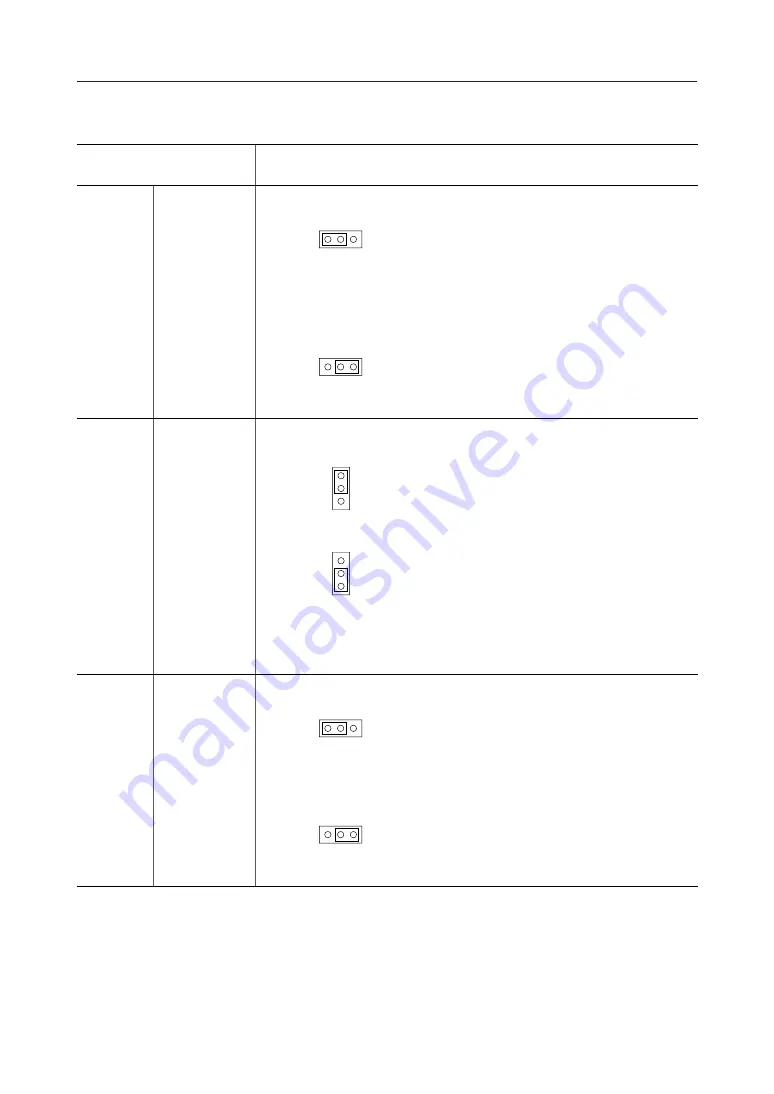
SYNC2 SEL
JP11
Jumper pins for setting SYNC2 (channel 2 SYNC) input.
SCK SEL
JP12
Jumper pins for setting SCK input (channel 1 and channel 2 are common).
CLKIN SEL
JP13
Jumper pins for switching the oscillator circuit used as the MSM7617's CLKIN input.
External input mode:
The external sync signal from the EXT.SYNC2 pin will
be used for SYNC2. SYNC2 and SCK must be
synchronized, so if EXT.SYNC2 is used then SCK
must also be input externally.
Internal input mode:
The sync signal set by JP10 (INT.SYNC2) will be used
for SYNC2.
Internal mode:
Depending on the setting of JP20 (INT SCK SEL), either
the internal SCK (SCKO) or the SCK generator's SCK
signal will be used for SCK.
External mode:
The SCK signal input from the EXT.SCK pin will be
used for SCK. SCK and SYNC must be synchronized,
so SYNC1 and SYNC2 must also be input externally.
OSC mode:
The OSC1 (crystal oscillator) will be used for CLKIN.
This mode is not used because OSC1 (liquid
crystal oscillator) is not mounted on the board.
X'tal mode:
The Y1 (crystal resonator) oscillator output will be
used for CLKIN.
EXT/INT
JP11
EXT/INT
JP11
JP13
JP13
OSC1/X'tal
OSC1/X'tal
JP12
INT/EXT
SCK
JP12
INT/EXT
SCK