


NXP Semiconductors
UM11711
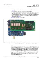
PCAL6524EV-ARD evaluation board
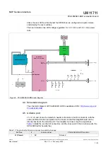
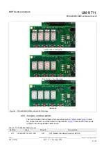
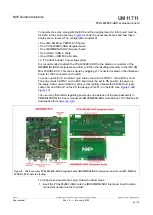
drives the user LEDs, while the last four MSB lines are configured as inputs and are
controlled by the user switches.
The board contains two LDO voltage regulators, for 3.3 V (U3) and 1.8 V (U4), power
rails.
Figure 2. PCAL6524EV-ARD block diagram
4.4 Schematic diagram
The schematic diagram of PCAL6524EV-ARD is available at URL:
.
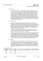
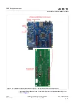
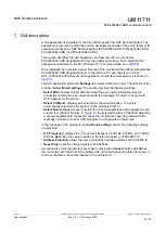
4.5 Arduino port
J1, J2, J3, and J4 are the mated pin headers of Arduino Uno R3 connectors, with the
same electrical function and placed on the board, so that the daughterboard can be
directly inserted in the Arduino port. The daughter card uses only five signal lines.
details the pin chart of connectors, and the lines used in the circuit (see also the
SPF-46658.pdf schematic file).
Ref Des
#
Arduino label
PCAL6524EV-ARD function
J1 (Power)
1
NC
Not used
Table 1. The pin chart of Arduino connectors and their usage
UM11711
All information provided in this document is subject to legal disclaimers.
© NXP B.V. 2022. All rights reserved.
User manual
Rev. 1.0 — 19 January 2022
7 / 30