NXP Semiconductors LPC8N04 User Manual Download Page 14

UM11082

All information provided in this document is subject to legal disclaimers.

© NXP B.V. 2018. All rights reserved.

User Manual

Rev. 1.1 — 12 January 2018 

14 of 18


NXP Semiconductors

LPC8N04 Development Board

User Manual

4.1  Using an external debug probe

An external debug probe that supports ARM’s SWD interface, such as a SEGGER J-Link 
or PE Micro probe, can be used with the LPC8N04 Development Board board. The 
external probe must be connected J1. When an external debug probe is used, the 
on-board probe must be held in reset by placing a jumper on P1. It is recommended that 
P1 is fitted before powering the board.
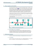
5. Expansion 

connectors/headers

All the usable I/O signals from the LPC8N04 Target are routed to the P4 header, along 
with a reset signal and 3.3V power. 12 I/Os are shared with the 5x7 LED array, including 
the two SWD signals (PIO0_11 and PIO0_10), and PIO0_3 which is shared with the 
speaker driver. These three signal may be disconnected for all these functions using P7, 
P8 and P9; for other I/Os to be used the MP and DP sections must be separated or the 
560 ohm LED row resistor (R26, R27, R29, R32, R36, R37 or R38) removed. For further 
details please refer to the board schematics.

Header P4 is designed to accept either a Grove I2C connector or PMod 6 pin SPI Type 2 
connector, for easy connection of off-the-shelf sensors

5.1  Main expansion connectors (DP Board P3, MP Board P4)

The 


Table 2.

Arduino expansion connector pin mappings (CN3)

P3 pin P4 pin LPC8N04 pin

PMod connection Grove connection

1

2

PIO0_0 (LED ROW5 / User Button)

2

1

PIO0_4 (LED COL2)

SCL

3

4

PIO0_1 (LED ROW4)

4

3

PIO0_5 (LED COL1)

SDA

5

6

PIO0_3 (SPKR/LED ROW6)

6

5

VCC

VCC

VCC

7

8

PIO0_7 (LED ROW1)

8

7

GND

GND

GND

9

10

PIO0_10 (SWCLK / LED COL3)

10

9

PIO0_6 (LED COL0)

SCK

11

12

PIO0_11 (SWDIO / LED COL4)

12

11

PIO0_9 (LED ROW3)

SDO

13

14

nc

14

13

PIO0_8 (LED ROW2)

SDI

15

16 RESET

16

15

PIO0_2 (LED ROW0)

SSEL

Summary of Contents for LPC8N04

Page 1: ...anual Rev 1 1 12 January 2018 1 of 18 NXP Semiconductors LPC8N04 Development Board User Manual UM11082 User Manual for LPC8N04 Development Board Rev 1 1 12 January 2018 User Manual Document informatio...

Page 2: ...NXP B V 2018 All rights reserved User Manual Rev 1 1 12 January 2018 2 of 18 NXP Semiconductors LPC8N04 Development Board User Manual Revision history Rev Date Description 1 0 20171218 First draft 1...

Page 3: ...ker LS1 The LPC8N04 Development Board board includes the following features Compatible with MCUXpresso IDE and other popular toolchains incl IAR and Keil Detachable two section board featuring minimal...

Page 4: ...the layout of the LPC8N04 Development Board board indicating location of jumpers buttons connectors expansion options and MCU devices Fig 2 Board layout top silkscreen SWD LED jumpers P8 P7 SPKR LED j...

Page 5: ...P1 when using this header 4 1 S1 LPC8N04 power on off switch When the switch is open the power is disconnected from the LPC8N04 This switch is provided to prevent accidental draining of the batteries...

Page 6: ...r see installation notes included in the package for further information 3 2 Running the out of box demo The LPC8N04 on the Development Board is pre programmed with a demonstration program which desig...

Page 7: ...enabled on the smartphone then activate the App Tap on the LED TEXT AND MUSIC tab at the top left then the Read NDEF button 3 2 2 Enabling and reading the and scrolling message temperature Bring the p...

Page 8: ...essage in the Text box then tap Write NDEF to write the message to the LPC8N04 The message TAG successfully written should appear along with the speed at which the write took place The LED array will...

Page 9: ...instead of the top row of LEDs see Figure 3 By default the firmware will assume this GPIO is being used for the LED row but will switch to driving the speaker once a push of button S2 is detected Beca...

Page 10: ...Semiconductors LPC8N04 Development Board User Manual 3 2 5 Running demos using energy harvesting If a smart phone with sufficient NFC reader power is used a demo can be run using energy harvesting to...

Page 11: ...DAP protocol This protocol is supported by MCUXpresso IDE and other popular IDEs such as Keil MDK and IAR EWARM It is not normally necessary to update the debug probe firmware but this can be done by...

Page 12: ...click in Import a new project from the file system 4 In the Import project s from file system dialog box that opens click Browse in the Project Archive from zip section and select the LPC8N04 code zi...

Page 13: ...File Explorer or equivalent on Mac Linux platforms look at the available drives on your system A device called CRP_DISABLED will appear 4 Delete the firmware bin file on the CRP_DISABLED drive 5 Drag...

Page 14: ...signals PIO0_11 and PIO0_10 and PIO0_3 which is shared with the speaker driver These three signal may be disconnected for all these functions using P7 P8 and P9 for other I Os to be used the MP and DP...

Page 15: ...that energy harvesting can still operate when the power switch is set in the off position Protection diodes are provided to prevent reverse powering of the coin cell batteries or external debug probe...

Page 16: ...th a scanning technique is provided in the app_demo example code mentioned in Section 3 3 7 3 Speaker and Speaker Driver A surface mount speaker LS1 is provided on the reverse side of the DP section o...

Page 17: ...be expected to result in personal injury death or severe property or environmental damage NXP Semiconductors accepts no liability for inclusion and or use of NXP Semiconductors products in such equip...

Page 18: ...7 3 2 3 Updating the scrolling message 8 3 2 4 Playing a tune 9 3 2 5 Running demos using energy harvesting 10 3 3 Setting up the board for Development 11 3 3 1 Using MCUXpresso IDE using on board de...

Reviews: