NXP Semiconductors KITUSBSPIEVME User Manual Download Page 4

USB to SPI Interface Evaluation Board, Rev. 1.0

4

Freescale Semiconductor

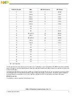
This connector mates with the MON08 cable provided with the P & E Cyclone Pro or Freescale FSICEBASE programmer.
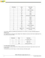
USB Connector

A “B” type USB connector is provided to allow a standard “A to B” USB cable to interconnect the PC to the Evaluation Board. The 
pinout of this connector is as follows:

VCC and Oscillator Jumper Selects

Two separate three pin jumpers, labeled JP1 and JP2 are provided to allow the selection of power and clock source for the 
Evaluation Board.

JP1 selects the source of the VCC power (+5 volts) in accordance with the following table:

Pin Number

Name

Description

1

NC

Unused

2

GND

VSS (System Gnd)

3

NC

Unused

4

RST

Reset

5

NC

Unused

6

IRQB

Interrupt Request (Low active)

7

NC

Unused

8

NC

Unused

9

NC

Unused

10

PTA0

Port A Bit 0

11

NC

Unused

12

PTA1

Port A Bit 1 

13

OSC

4.9152 MHz Oscillator

14

PTA2

Port A Bit 2

15

MON08_VCC

+5 Volts from P & E or FSICE 

16

PTC1

Port C Bit 1

Pin Number

Name

Description

1

+5

+5 Volts from the PC

2

D-

Signal - line

3

D+

 line

4

GND

System ground (VSS)

Summary of Contents for KITUSBSPIEVME

Page 1: ...SBSPIEVME Evaluation Board is a working hardware software example that allows a user to become familiar with the MCHC908JW32FC by means of an actual useful application a USB to SPI and USB to parallel...

Page 2: ...is included on the accompanying CD LED Display The LED s are provided as a visual output device for debugging and test purposes As configured from the factory LED 2 indicates when power is applied and...

Page 3: ...pin outs for the SPI signals and Control and Data signals by using shorting jumper plugs or wire jumpers Consult the specific Freescale Evaluation Board documentation for the correct signal pin defin...

Page 4: ...d JP1 and JP2 are provided to allow the selection of power and clock source for the Evaluation Board JP1 selects the source of the VCC power 5 volts in accordance with the following table Pin Number N...

Page 5: ...acitors C2 and C3 27 pf and resistor R4 10M provide the operating clock source for the JW32 The 4 000 MHz clock is used as a reference for the PLL in the JW32 The internal bus frequency is 8 MHz and t...

Page 6: ...ces of software were licensed from Thesycon a software development company in Germany All of the source code that is available is provided on the Installation CD in a directory called source For an ex...

Page 7: ...ries to the P E Cyclone Pro programmer via the MON08 port to re Flash the JW32 The documentation for this process is contained in the CodeWarrior suite of tools and the P E documentation global h Some...

Page 8: ...y of its products for any particular purpose nor does Freescale Semiconductor assume any liability arising out of the application or use of any product or circuit and specifically disclaims any and al...

Reviews: