


Optical Mouse Transmitter
Designer Reference Manual
DRM050 — Rev 0
18
Optical Mouse Transmitter
MOTOROLA
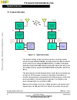
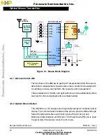
Figure 3-1. Mouse Block Diagram
3.2.1 Microcontroller JB8
The functions of the JB8 are to get the XY displacement from the sensor,
detect the Z displacement, check button status, control the baseband IC
to sending out data, and perform the overall power management.
Three standard left, middle, and right buttons (and two additional buttons
reserved for future development) are implemented.
3.2.2 Optical Mouse Sensor
The AN2030 is a 3-V supply sensor specially design for wireless optical
mouse. The communication between the sensor and the JB8 is through
Serial Peripheral Interface with clock input at the SCLK pin and
bidirection data interface at SDIO pin. The Power Down (PD) pin is used
to power down the sensor when it’s not in use.
ADNS-2030
SCLK
SDIO
PD
XY_LED
IMAGE
SENSOR
(16-pin PDIP)
MC68HC908JB8
Buttons
PTA0
L
M
R
PTA1
PTE0
PTA6
PTA5
PTA2
Z1
(44-pin QFP)
PTE1
PTE2
DATA BUS
ADDRESS / CTL BUS
PTB7-PTB0
PTC7-PTC0
2.4 GHz RF
Transceiver
Module
LOOP
ANTENNA
DGND
L2
R2
PTA4
PTA3
Z2
Baseband
MAC IC
D100
DC/DC Converters
3.3V and 5V
OSC1
OSC2
RST
6MHz
30pF
30pF
X1
100nF
10M
RFD_INT
IRQ
Z-axis
Encoder
F
re
e
sc
a
le
S
e
m
ic
o
n
d
u
c
to
r,
I
Freescale Semiconductor, Inc.
For More Information On This Product,
Go to: www.freescale.com
n
c
.
..