background image


2013

09

27

NUR

05WL2


Implementation


Guide


v1.1


This


pin


is


used


for


module


UART


input


signal.


Logic


level


is


3.3V.


If


UART


is


used


for


communication


the


pin


should


be


connected


to


the


Host


MCU


serial


TX


port.


Signal


name:


TX


Pin


number(s):


9


This


pin


is


used


for


module


UART


output


signal.


Logic


level


is


3.3V.


If


UART


is


used


for


communication


the


pin


should


be


connected


to


the


Host


MCU


serial


RX


port.


Signal


name:


USB_DN


Pin


number(s):


10


This


pin


is


used


as


USB_D

‐ 

device


port.


It


is


advised


to


use


external


ESD


protection


component


if


connected


to


user


accessible


USB


connector.


Signal


name:


USB_DP


Pin


number(s):


11


This


pin


is


used


as


USB_D+


device


port.


It


is


advised


to


use


external


ESD


protection


component


if


connected


to


user


accessible


USB


connector.


Signal


name:


USB_DET


Pin


number(s):


12


This


pin


is


only


used


for


USB


connection


detection.


It


is


advised


to


use


external


ESD


protection


component


if


connected


to


user


accessible


USB


connector.


Current


is


not


drawn


from


this


input


pin.


Signal


name:


VCC_3V3_OUT


Pin


number(s):


13


This


pin


is


connected


to


internal


power


regulator


output.


The


pin


is


used


for


production


testing


and


it


should


not


be


used.


Signal


name:


MODULE_EN


Pin


number(s):


14


Driving


this


pin


to


high


will


enable


the


NUR

05WL2


module.


It


is


internally


connected


to


onboard


voltage


regulator’s


enable


input.


The


trigger


level


is


1.2V


and


the


reader


module


will


wake


up


in


50ms.


If


the


external


power


switch


is


used


to


toggle


ON


and


OFF,


this


pin


can


be


connected


directly


to


VCC_3V6_IN.


Signal


name:


NC


Pin


number(s):


16,


31,


32


These


pins


are


internally


not


connected.


Signal


name:


VCC_3V6_IN


Pin


number(s):


17


This


pin


is


used


for


power


supply


input


for


NUR

05W


module.


It


is


recommended


to


use


200µF


(low


ESR)


100nF


and


100pF


capacitor


near


the


VCC_3V6_IN


input


pin


to


maintain


stable


operating


voltage


for


the


reader


module.


Signal


name:


RFU


Pin


number(s):


1,


18,


19


These


pins


are


reserved


for


future


use.


Do


not


connect


these


pins.


Signal


name:


GND/RF_DIF


Pin


number(s):


29


This


pin


is


internally


connected


to


GND.


It


is


reserved


for


future


use


as


secondary


RF


output.


Summary of Contents for NUR-05WL2

Page 1: ...2013 09 27 NUR 05WL2 Implementation Guide v1 1 NUR 05WL2 IMPLEMENTATION GUIDE ...

Page 2: ...ion Date Author Remarks 0 1 2 1 2013 Toni Heijari initial version 0 2 6 3 2013 Toni Heijari minor additions 0 3 4 4 2013 Toni Heijari changed sections 1 3 and 4 1 1 0 12 6 2013 Toni Heijari first released version 1 1 2 9 2013 Toni Heijari Changed section 11 2 and 11 3 ...

Page 3: ... 3 3 Signal description 10 4 OEM DESIGN CONSIDERATIONS 12 4 1 RF output and antenna requirements 12 4 2 Power supply 12 4 3 USB device port 13 5 RF PARAMETERS 14 5 1 TX level 14 5 2 Receiver sensitivity 14 5 3 Leakage cancellation 14 5 4 Modulation 15 5 5 Link frequency 15 5 6 RX encoding Miller encoding 15 5 7 Region 16 6 READING PARAMETERS 18 6 1 Q value 18 6 2 Session 18 6 3 Rounds 19 6 4 Selec...

Page 4: ...torage conditions 31 10 2 Soldering process 32 11 REGULATORY AGENCIES INFORMATION 34 11 1 European Union and EFTA countries 34 User s Guide Requirements 34 Labeling Requirements 37 Approved Antennas 37 11 2 FCC 38 User s Guide Requirements 39 Labeling Requirements 39 Approved Antennas 40 11 3 Industry Canada 40 Labelling Requirements for the Host device 41 Certified Antennas 41 11 4 Industrie Cana...

Page 5: ...m sensitivity is 80dBm 1 1 BLOCK DIAGRAM 1 2 KEY FEATURES SMT compatible module with extremely small footprint ISO 18000 6C EPC C1G2 full protocol support custom commands Low power consumption with high noise rejection DRM compatible High performance with 27dBm output power adjustable by 1dB steps Approved by ETSI FCC and IC telecommunication organizations Selectable RF parameters RX coding link f...

Page 6: ... 1 3 TYPICAL APPLICATION SCHEMATICS Typical application schematic including USB connection with ESD protection circuitry 2 GPIO outputs for LED indicators GPIO trigger input NUR 05WL2 module and MMCX antenna connector A simple application schematic ...

Page 7: ...C CHARACTERISTICS Typical values VCC_3V6_IN 3 6V 25 C Symbol Parameter Min Typ Max Units Vext Supply voltage 3 4 3 6 5 5 V Iext Supply current 0 8A 1A mA Isource GPIO source current 3 mA Isink GPIO sink current 6 mA Vlow GPIO input low level voltage 0 8 V Vhigh GPIO input high level voltage 2 0 V Ven Module enable voltage 1 2 Supply V 2 3 RF CHARACTERISTICS Typical values VCC_3V6_IN 3 6V 25 C Symb...

Page 8: ...e frequency may decrease the performance Also the tag antenna and the tag IC may have significant effect on the values presented below Also selected radio and inventory parameters have got a big influence to reading performance Typical values VCC_3V6_IN 3 6V 25 C Symbol Parameter Min Typ Max Units Rdist Typical reading distance with 5 dBi antenna 5 m Rrate Typical reading rate 200 tags s Otemp Ope...

Page 9: ...ectional RFU do not connect 2 GPIO_5 Bidirectional 3 3V GPIO 3 GPIO_4 Bidirectional 3 3V GPIO 4 GPIO_3 Bidirectional 3 3V GPIO 5 GPIO_2 Bidirectional 3 3V GPIO 6 GPIO_1 Bidirectional 3 3V GPIO 7 ERASE Input DNU do not use 8 RX Input Data from Host to Module 9 TX Output Data from module to Host 10 USB_DN Bidirectional USB device port 11 USB_DP Bidirectional USB device port ...

Page 10: ...al 50Ω RF output input 28 GND Supply input Ground 29 GND RF_DIF Bidirectional RFU do not connect 30 GND Supply input Ground 31 NC Not connected internally not connected 32 NC Not connected internally not connected 33 41 GND Supply input Ground 3 3 SIGNAL DESCRIPTION Signal name GND Pin number s 15 20 26 28 30 33 41 These pins are used for grounding and to improve the thermal performance They shoul...

Page 11: ...SB connector Current is not drawn from this input pin Signal name VCC_3V3_OUT Pin number s 13 This pin is connected to internal power regulator output The pin is used for production testing and it should not be used Signal name MODULE_EN Pin number s 14 Driving this pin to high will enable the NUR 05WL2 module It is internally connected to onboard voltage regulator s enable input The trigger level...

Page 12: ...eceiver because of the TX power reflecting back from the antenna In the NUR 05WL2 module there is also an automatic leakage cancellation system that decreases the effect of the reflected signal and it also improves the isolation of the RX signal from the TX signal The automatic leakage cancellation can be triggered using SW API command For further information on the leakage cancellation see the se...

Page 13: ...e at the time Connecting the USB will automatically prevent communication via serial port It is advised to use external ESD protection component if connected to user accessible USB connector Below is the typical schematics used with NUR 05WL2 module Typical schematics for USB connection with ESD protection Used components Ref Description Manufacturer Part code U15 ESD protection ST Microelectronic...

Page 14: ...23 200 14 13 20 5 22 158 15 12 16 6 21 126 16 11 13 7 20 100 17 10 10 8 19 79 18 9 8 9 18 63 19 8 6 5 2 RECEIVER SENSITIVITY The maximum LBT sensitivity is of 80dBm The receiver can handle 5dBm of power reflecting back to RF_OUT pin without having a big impact on the performance Tolerance to reflecting signal can be significantly increased using NUR 05WL2 leakage cancellation functionality The rec...

Page 15: ...t the frequency of reader transmission frequency 256 kHz The selectable parameters are 160 kHz 256 kHz and 320 kHz Tags that are compliant with ISO18000 6C EPC C1G2 must support all these parameters The link frequency also affects tag to reader data rate which is calculated by formula below Tag to reader data rate Link frequency Miller coding By default the link frequency is set to 256 kHz 256 kHz...

Page 16: ... default Miller 4 is used In addition to miller schemes also FM0 encoding is supported In this case link frequency directly determines the tag to reader data rate Table describing different data rates Link frequency kHz RX encoding Tag to reader data rate kbps 160 FM0 160 160 M2 80 160 M4 40 160 M8 20 256 FM0 256 256 M2 128 256 M4 64 256 M8 32 320 FM0 320 320 M2 160 320 M4 80 320 M8 40 5 7 REGION ...

Page 17: ...bed below Table describing custom hop table parameters Parameter Value Description Frequency entry 840 000 960 000 kHz Defines the center frequency of the first transmit channel Channel count 1 100 Defines the number of transmit channels Channel spacing 25 n kHz Defines the frequency between transmit channels Channel time minimum 100 ms Defines the time that reading is ON at the same channel Wait ...

Page 18: ...512 2 4 10 1024 3 8 11 2048 4 16 12 4096 5 32 13 8192 6 64 14 16384 7 128 15 32768 6 2 SESSION There are four session options which you can use when initializing inventory round Every session has two target states A and B By default Gen2 tags are at state A if tag has not been read recently When tag is read it flips to state B and doesn t reply to readers query The table below describes the persis...

Page 19: ...utomatic adjustment decides after every query round whether another round is necessary based on the number of data collisions By default rounds setting is set to 0 This setting can help the reader to find all the tags that are in the readers reading field when using session 0 Because tags that are found in query round 1 doesn t replay in the following query rounds When using session 1 2 3 this doe...

Page 20: ...unds value than 1 to be able to find all the individual tags By default automatic 0 rounds setting is used Other settings like modulation link frequency and RX encoding has a minor impact to the reading speed of the reader When operating in optimal environment following will apply RX encoding FM0 is fastest but quite sensitive to interferences M8 slowest but very robust Modulation No effect to spe...

Page 21: ... how the NUR 05W module GPIOs can be configured I O Function Action Trigger Output Output RFON Output RFIDREAD Output Beeper Output Antenna control 1 Output Antenna control 2 Input Input Notify rising falling both Input Scantag rising falling both Input Inventory rising falling both RFON GPIO type OUTPUT When GPIO is configured as RFON it drives high state always when power amplifier is turned on ...

Page 22: ... end of reading and last found tag can be configured Scantag GPIO type INPUT When GPIO is configured as scan tag reader will perform just one read Triggering can be configured to be from falling rising both edges Notify GPIO type INPUT When GPIO is configured as notify will reader send notification to Host application when triggered by selected GPIO Triggering can be configured to be from falling ...

Page 23: ...2013 09 27 NUR 05WL2 Implementation Guide v1 1 Case selected antenna antenna control 1 antenna control 2 0 antenna 1 low low 1 antenna 2 high low 2 antenna 3 low high 3 antenna 4 high high ...

Page 24: ...power value that is leaking into the receiver due to imperfect coupler isolation or antenna mismatch 8 2 CHANNEL SCANNER This function can be used to monitor the interferences in the current frequency band It is also useful if you want to check if some fixed channel is in use When you trigger this function NUR 05WL2 will scan all the channels in current region and return the RSSI value of each cha...

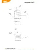
Page 25: ...2013 09 27 NUR 05WL2 Implementation Guide v1 1 9 DIMENSIONS 9 1 MECHANICAL DIMENSIONS ...

Page 26: ...2013 09 27 NUR 05WL2 Implementation Guide v1 1 ...

Page 27: ...2013 09 27 NUR 05WL2 Implementation Guide v1 1 9 2 LAND PATTERN ...

Page 28: ...2013 09 27 NUR 05WL2 Implementation Guide v1 1 9 3 PASTE STENCIL ...

Page 29: ...2013 09 27 NUR 05WL2 Implementation Guide v1 1 9 4 PACKING TRAY DIMENSIONS ...

Page 30: ...2013 09 27 NUR 05WL2 Implementation Guide v1 1 All measures are in mm ...

Page 31: ...int The board assembly process of NUR module on motherboard will introduce re flow of module components Thus to avoid degradation of solder joint interfaces the module has to be stored and soldered according to the guidelines given below 10 1 STORAGE CONDITIONS Long term storage Store modules in unopened vacuum packs in a dry cabinet under following environmental conditions Temperature 15 27 C opt...

Page 32: ... C due to higher mp and lower fluidity of non eutectic SnAgCu alloys This will increase thermal stress to module and motherboard greatly Convection reflow oven heater configuration Double sided heating required in reflow recommended in preheating zones Maximum absorbed moisture content prior to thermal processing 0 1 w Test method IPC TM 650 2 6 28 Moisture content and or moisture absorption rate ...

Page 33: ...oldering phase total duration 190s max time above 217 C mp 30s Tpeak max 235 C measured at module bottom Tpeak max 225 C measured at motherboard surface under module Cooling Two stage double sided cooling recommended 1st stage 2 5 C s cooling until melting point 2nd stage 1 3 C s after melting point ...

Page 34: ...s effort that the device with the integrated NUR 05WL2 module is in compliance with the requirements 11 1 EUROPEAN UNION AND EFTA COUNTRIES USER S GUIDE REQUIREMENTS This apparatus is in compliance with the essential requirements of the R TTE Directive 1999 5 EC In order to prove presumption of conformity with the essential requirements of the R TTE Directive 1999 5 EC the following requirements a...

Page 35: ...tus vastavust direktiivi 1999 5 EÜ põhinõuetele ja nimetatud direktiivist tulenevatele teistele asjakohastele sätetele English Hereby name of manufacture declares that this type of apparatus is in compliance with the essential requirements and other relevant provisions of Directive 1999 5 EC Español Spanish Por medio de la presente name of manufacture declara que el type of apparatus cumple con lo...

Page 36: ...statas Nederlands Dutch Hierbij verklaart name of manufacture dat het toestel type of apparatus in overeenstemming is met de essentiële eisen en de andere relevante bepalingen van richtlijn 1999 5 EG Malti Maltese Hawnhekk name of manufacture jiddikjara li dan type of apparatus jikkonforma mal ħtiġijiet essenzjali u ma provvedimenti oħrajn relevanti li hemm fid Dirrettiva 1999 5 EC Magyar Hungaria...

Page 37: ... koskevien direktiivin muiden ehtojen mukainen Svenska Swedish Härmed intygar name of manufacture att denna type of apparatus står i överensstämmelse med de väsentliga egenskapskrav och övriga relevanta bestämmelser som framgår av direktiv 1999 5 EG LABELING REQUIREMENTS The CE marking must be in a visible area on the OEM product APPROVED ANTENNAS Maximum allowed ERP power is 33dBm NUR 05WL2 has o...

Page 38: ...es with Part 15 of the FCC Rules Operation is subject to the following two conditions 1 This device may not cause harmful interference and 2 this device must accept any interference received including interference that may cause undesired operation FCC Caution Any changes or modifications not expressly approved by the party responsible for compliance could void the user s authority to operate this...

Page 39: ...garding how to install or remove this RF module in the user manual of the end product For the User s Guide the required FCC statements outlined in the User s Guide Requirements section must be in a prominent location USER S GUIDE REQUIREMENTS To comply with FCC s RF radiation exposure requirements the antenna s used for this transmitter must be installed such that a minimum separation distance of ...

Page 40: ...e complies with Industry Canada licence exempt RSS standard s Operation is subject to the following two conditions 1 this device may not cause interference and 2 this device must accept any interference including interference that may cause undesired operation of the device Under Industry Canada regulations this radio transmitter may only operate using an antenna of a type and maximum or lesser ga...

Page 41: ...ed although the OEM integrator shall demonstrate that the end product is in compliance with the other regulatory requirements There is no user s documentation requirements other than that the required FCC statements outlined in the FCC section are in a prominent place in the user s guide LABELLING REQUIREMENTS FOR THE HOST DEVICE The end product must be labeled with the following identification in...

Page 42: ...ntégrateurs OEM sous les conditions suivantes 1 La ou les antenne s doivent être installées à une distance de separation minimum de 20cm celle ci doit être maintenue entre le radiateur antenne et le s utilisateur s ou toute s autre s personne s a tout moment 2 Le module transmetteur ne doit pas être colocalisé avec d autre s transmetteur s sauf si ce s dernier s répond ent avec ceux qui sont dans ...

Page 43: ...7 NUR 05WL2 Implementation Guide v1 1 Option 1 Fabricant Nordic ID Déscription de l antenne Circular polarized patch antenna Portée de la fréquence 902 928 MHz Numéro de la pièce du fabricant Sampo S0 Gain 7dBi ...

Reviews: