Specifications
5
13
14
MODE0
MODE1
The MODE0 and MODE1 pins control the mode of the unit as
follows:
MODE0
MODE1
Description
0
0
Step/Direction Mode:
Digital mode
where DIR+/A controls direction
(high=clockwise, low=counterclockwise)
and the falling edge of PULSE/B initiates
each step.
1
0
Quadrature Mode:
Digital mode where
pulses are generated from edge
transitions of both the A-phase (DIR+/A)
and B-phase (PULSE/B) inputs.
0
1
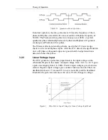
Linear Voltage Input Mode:
Analog
mode where ANALOG IN+ controls pulse
direction and rate. Negative voltage
results in counter-clockwise motion:
positive results in clockwise. See Figure
11 for the frequency-to-voltage
correlation.
1
1
Bang-Bang Voltage Input Mode:
Analog mode where voltage on ANALOG
IN+ above the threshold results in
maximum analog pulse rate. Polarity
controls direction.
Mode bits are only read when power is turned on. They are not
optically isolated. Tie them to +5V OUT or SYS GROUND.
15
LIDLE
Opto-coupled TTL input. Low input disables pulse generation and
reduces power consumption. Can also be used as system interlock.
16
LFAULT
Open-collector opto-coupler output pulled low when output amplifier
temperature limit is exceeded. On start-up, firmware version
number is present on this pin in the form of on/off pulses.
17
N/C
Not connected pin.
18
+5V REF
Reserved. Test point for manufacturing reference only.
19
LV PULSE
Reserved. Test point for manufacturing reference only.
20
-15V
Reserved. Test point for manufacturing reference only.
21
TEMP MONITOR
Voltage proportional to the output-amplifier case temperature. If it
goes above 4 V pulls LFAULT low.


