National
Semiconductor
December 2005
Rev 5
Evaluation Board Instruction Manual
ADC08100 8-Bit, 20 Msps to 130Msps, Analog-to-Digital
Converter with Internal Sample & Hold
© 2002, 2005 National Semiconductor Corporation.
1
http://www.national.com
Page 1: ...uctor December 2005 Rev 5 Evaluation Board Instruction Manual ADC08100 8 Bit 20 Msps to 130Msps Analog to Digital Converter with Internal Sample Hold 2002 2005 National Semiconductor Corporation 1 http www national com ...
Page 2: ... Blank Page 2 http www national com ...
Page 3: ...rd 7 5 1 Software Installation 7 5 2 Setting up the ADC08100 Evaluation Board 7 5 2 1 Board Set up 7 5 2 1 1 Computer Mode Operation 7 5 2 1 2 Manual Mode Operation 7 5 2 2 Quick Check of Analog Functions 7 5 2 3 Quick Check of Software and Computer Interface Operation 8 5 2 4 Getting Consistent Readings 8 5 2 5 Jumper Information 8 5 2 6 Troubleshooting 9 6 0 Evaluation Board Specifications 9 7 0...
Page 4: ... Blank Page 4 http www national com ...
Page 5: ...ference voltage VRT for the ADC to 1 9V at TP2 Use VR2 to set the bottom reference voltage VRB for the ADC to 0 3V at TP4 4 Connect the jumper at J4 to pins 1 and 2 those farthest from oscillator Y1 5 Connect a signal of 1 6VP P amplitude from a 50 Ohm source to Analog Input BNC J2 The ADC input signal can be observed at TP7 Because of isolation resistor R17 and the scope probe capacitance the inp...
Page 6: ...igitized should be applied to BNC connector J2 This 50 Ohm input is intended to accept a low noise sine wave signal of 1 5V peak to peak amplitude To accurately evaluate the ADC08100 dynamic performance the input test signal should be passed through a high quality bandpass filter 60dB minimum stop band attenuation as even the best generators do not provide a pure enough sine wave to properly evalu...
Page 7: ...efault position as shown in Figure 1 to divide the clock oscillator frequency by two for the ADC08100 3 Connect power to the board per requirements of section 4 6 and confirm that Red LED D4 on the ADC08100 evaluation board and D1 on the Digital Interface board are on indicating clock presence 4 6 Power Requirements 4 Connect The ADC08100 evaluation board to Digital Interface Board WAVEVSN RD 3 0 ...
Page 8: ...e from the same generator whatever frequency instability jitter is present in the two signals will cancel each other 4 RUN program WAVEVSN2 EXE 5 After turning on power be sure to wait for yellow LED D4 on the Digital Interface Board to go out before trying to acquire data or the board will freeze and you will have to cycle the power Windowing an FFT Option under WaveVision should be turned off fo...
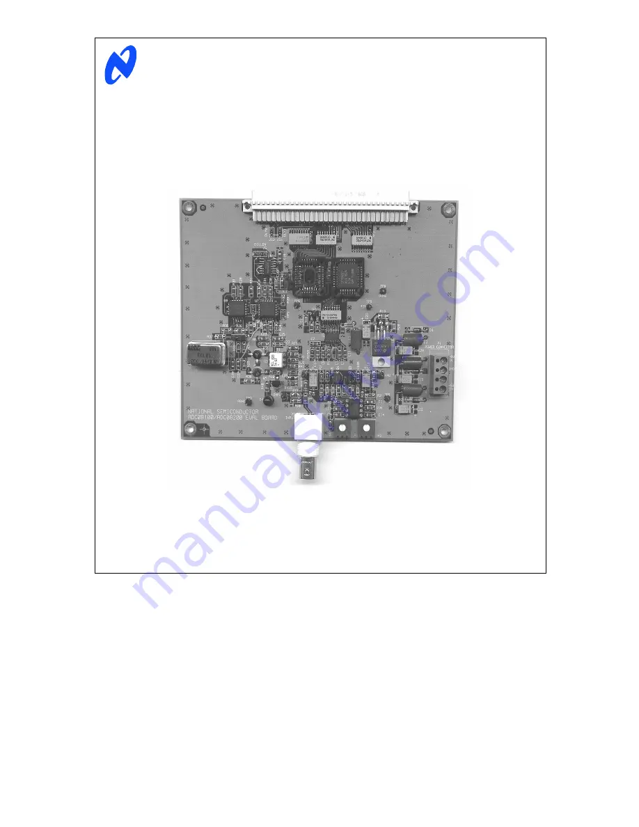
Page 9: ...D3 of the Digital Interface Board are on See the Digital Interface Board manual for their functions Problem Opening Comm Port or Error Setting Comm State errors mean that the comm port selected is not the one to which the eval board is connected 6 0 Evaluation Board Specifications Be sure cable connections are solid Board Size 5 x 7 12 7cm x 17 8 cm Be sure that the board to computer cable is not ...
Page 10: ...uF 6 3V R10 1k R11 1k R12 100 R10A 47 C9 1uF R9 47 C16 1uF TP2 VRT C2 1uF C5 1uF C12 1uF C15 1uF C17 OPEN R15A 130 R15 220 C17A 1uF R16 47 R18 51 TP7 INPUT R17 100 C17B 1uF R1 10k R4 100 C1 100pF ADC0 ADC1 ADC2 ADC3 ADC4 ADC5 ADC6 ADC7 R13 470 C18A 47pF JS1 DLY1 C6 1uF 5V C7 1uF D0 D1 D2 D3 D4 D5 D6 D7 JS2 DLY1 C18 1uF J3 96 Pin Female Q4 Q3 Q2 Q1 Q0 FF EF 5 6 7 8 9 10 11 12 13 29 28 27 26 25 24 2...
Page 11: ...4 9 12 8 D CC __ CE VCC S Q _ Q R VEE 7 2 5 10 U8A MC10H131FN 19 18 13 12 14 D CC __ CE VCC S Q _ Q R VEE 15 20 17 10 U8B MC10H131FN R31 510 5V R38 510 5V 5V 5V R34 47 R36 47 R39 510 5V 5V 5V C28 1uF C30 1uF C31 1uF OUT __ IN IN 18 19 17 10 12 OUT __ IN IN 13 14 15 OUT __ IN IN 8 9 7 U7A MC10H125FN U7B MC10H125FN U7C MC10H125FN U7D MC10H125FN R28 47 R24 47 R26 510 5V C24 1uF 100MHz 2 50MHz 100MHz ...
Page 12: ...ype 1206 23 1 R6 1 8k 5 Type 1206 24 4 R7 R8 R10 R11 1k 5 Type 1206 25 1 R13 470 5 Type 1206 26 1 R15 220 5 Type 1206 27 1 R15A 130 5 Type 1206 28 1 R18 51 5 Type 1206 29 1 R19 2 00k 1 Type 1206 30 1 R20 3 01k 1 Type 1206 31 5 R21 R22 R33 R37 R40 330 5 Type 1206 32 5 R26A R26 R31 R38 R39 510 5 Type 1206 33 1 R27 130 5 Type 1206 34 1 R30 240 5 Type 1206 35 0 R41 Not Used n a 36 1 R41A 4 7k 5 Type 1...
Page 13: ...pply Connections J1 1 5V Positive Power Supply J1 2 GND Power Supply Ground J1 3 5V Logic and Digital Interface Board Supply J1 4 5 2V Negative Power Supply J1 Connector Number of Memory Chips Used hard wired Connect 1 2 One Memory Chip Default Connect 2 3 Two Memory Chips J2 and JP3 Not Used J4 Connector ADC Clock selection jumper settings Connect 1 2 Divide frequency of Y1 by 2 Default Connect 2...
Page 14: ... D5 C18 ADC output D6 B19 ADC output D7 C19 ADC output D8 not used ADC output D9 not used ADC output D10 not used ADC output D11 not used GND A1 thru A24 A28 B28 C28 A31 B31 C31 Memory Read Cock B25 Reserved Signal B22 C22 C23 Reserved Power A25 A26 B25 B26 C25 C26 5V Logic Power Supply to Digital Interface Board Reserved Power 5 2V A29 B29 C29 Reserved Power 5V A32 B32 C32 14 http www national co...
Page 15: ... Blank Page 15 http www national com ...
Page 16: ...ein 1 Life support devices or systems are devices or systems which a are intended for surgical implant into the body or b support or sustain life and whose failure to perform when properly used in accordance with instructions for use provided in the labeling can be reasonably expected to result in a significant injury to the user 2 A critical component is any component in a life support device or ...