background image

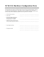
SCXI-1122 Hardware Configuration Form


Record the settings and revisions of your hardware and software on the line to the right of each item.  Complete a
new copy of this form each time you revise your software or hardware configuration, and use this form as a
reference for your current configuration.  Completing this form accurately before contacting National Instruments
for technical support helps our applications engineers answer your questions more efficiently.

SCXI-1122 Revision Letter

_____________________________________________________


Chassis Slot

_____________________________________________________


Grounding, Shielding, and Reference
Mode Selection (Factory Setting:
Parking position, W1, A-R0R1)

_____________________________________________________


SERDATOUT Resistor Pull-up Jumper
(Factory Setting: Enabled, W2, position 1)

_____________________________________________________


Other Modules in System

_____________________________________________________


_____________________________________________________


DAQ Boards Installed

_____________________________________________________


_____________________________________________________
 

Summary of Contents for SCXI-1122

Page 1: ...1993 1999 National Instruments Corporation All Rights Reserved User Manual Sixteen Channel Isolated Transducer Multiplexer Module for Signal Conditioning September 1999 Edition Part Number 320516B 01 SCXI 1122 TM ...

Page 2: ...o 905 785 0085 Canada Québec 514 694 8521 China 0755 3904939 Denmark 45 76 26 00 Finland 09 725 725 11 France 01 48 14 24 24 Greece 30 1 42 96 427 Germany 089 741 31 30 Hong Kong 2645 3186 India 91805275406 Israel 03 6120092 Italy 02 413091 Japan 03 5472 2970 Korea 02 596 7456 Mexico D F 5 280 7625 Mexico Monterrey 8 357 7695 Netherlands 0348 433466 Norway 32 27 73 00 Singapore 2265886 Spain Barce...

Page 3: ...CAUSED BY FAULT OR NEGLIGENCE ON THE PART OF NATIONAL INSTRUMENTS SHALL BE LIMITED TO THE AMOUNT THERETOFORE PAID BY THE CUSTOMER NATIONAL INSTRUMENTS WILL NOT BE LIABLE FOR DAMAGES RESULTING FROM LOSS OF DATA PROFITS USE OF PRODUCTS OR INCIDENTAL OR CONSEQUENTIAL DAMAGES EVEN IF ADVISED OF THE POSSIBILITY THEREOF This limitation of the liability of National Instruments will apply regardless of th...

Page 4: ...PART OF THE USER OR APPLICATIONS DESIGNER ADVERSE FACTORS SUCH AS THESE ARE HEREAFTER COLLECTIVELY TERMED SYSTEM FAILURES ANY APPLICATION WHERE A SYSTEM FAILURE WOULD CREATE A RISK OF HARM TO PROPERTY OR PERSONS INCLUDING THE RISK OF BODILY INJURY AND DEATH SHOULD NOT BE RELIANT SOLELY UPON ONE FORM OF ELECTRONIC SYSTEM DUE TO THE RISK OF SYSTEM FAILURE TO AVOID DAMAGE INJURY OR DEATH THE USER OR ...

Page 5: ...on 2 1 Digital Signal Connections 2 3 Analog Configuration 2 3 Current Loop Receivers 2 4 Hardware Installation 2 6 Chapter 3 Signal Connections 3 1 Front Connector 3 3 Front Signal Connection Descriptions 3 4 Analog Input Channel Signal Connections 3 5 Excitation Channel Signal Connections 3 8 Excitation Level 3 8 Using the Internal Half Bridge Completion 3 9 Temperature Sensor Connection 3 9 Rea...

Page 6: ...erview 5 1 Calibration Procedure 5 1 Calibration Equipment Requirements 5 1 Gain and Offset Calibration 5 2 Excitation Calibration 5 4 Appendix A Specifications A 1 Analog Input A 1 Excitation A 3 Physical A 3 Environment A 3 Appendix B Customer Communication B 1 Glossary Glossary 1 Index Index 1 ...

Page 7: ... and Averaging Rather Than Single Sample Channel Scanning 3 8 Figure 3 7 Connecting a Quarter Bridge Strain Gauge to Channel 0 3 9 Figure 3 8 SCXI 1122 Rear Signal Connector Pin Assignments 3 10 Figure 4 1 SCXI 1122 Block Diagram 4 2 Figure 4 2 Series Connection with Current Excitation 4 6 Figure 4 3 Four Wire Scan Connection with Multiplexed Current Excitation 4 6 Tables Table 2 1 Digital Signal ...

Page 8: ...escribes the optional software optional equipment and custom cables and explains how to unpack the SCXI 1122 Chapter 2 Configuration and Installation describes how to configure the SCXI 1122 jumpers and how to install the SCXI 1122 into the SCXI chassis Chapter 3 Signal Connections describes the input and output signal connections to the SCXI 1122 module via the SCXI 1122 front connector and rear ...

Page 9: ...mming examples and syntax examples This font is also used for the proper names of disk drives paths directories programs subprograms subroutines device names functions variables filenames and extensions and for statements and comments taken from program code NB NB refers to the NuBus series computers PC PC refers to the IBM PC XT the IBM PC AT and compatible computers SCXIbus SCXIbus refers to the...

Page 10: ...et up your hardware system use either the application software LabVIEW or LabWindows manuals or the NI DAQ manuals to help you write your application If you have a large and complicated system it is worthwhile to look through the software manuals before you configure your hardware Accessory manuals These are the terminal block and cable assembly installation guides They explain how to physically c...

Page 11: ...comments on our products and manuals We are interested in the applications you develop with our products and we want to help if you have problems with them To make it easy for you to contact us this manual contains comment and configuration forms for you to complete These forms are in Appendix B Customer Communication at the end of this manual ...

Page 12: ...DAQ board channel The SCXI 1122 operates with full functionality with the National Instruments MIO 16 Lab PC and the SCXI 1200 boards You can use the Lab and PC LPM 16 boards with the SCXI 1122 but these boards cannot scan the module These boards can perform only single channel reads You can multiplex several SCXI 1122s into a single channel thus greatly increasing the number of isolated analog in...

Page 13: ...ftware LabWindows has two versions LabWindows for DOS is for use on PCs running DOS and LabWindows CVI is for use on PCs running Windows and Sun SPARCstations LabWindows CVI features interactive graphics a state of the art user interface and uses the ANSI standard C programming language The LabWindows Data Acquisition Library a series of functions for using LabWindows with National Instruments boa...

Page 14: ...r or Workstation Figure 1 1 The Relationship between the Programming Environment NI DAQ and Your Hardware The National Instruments PC AT and MC Series DAQ boards are packaged with NI DAQ software for PC compatibles NI DAQ software for PC compatibles comes with language interfaces for Professional BASIC Turbo Pascal Turbo C Turbo C Borland C and Microsoft C for DOS and Visual Basic Turbo Pascal Mic...

Page 15: ...eed the register level programmer manual The SCXI 1122 Register Level Programmer Manual contains low level programming details such as register maps bit descriptions and register programming hints that you will need only for register level programming Some hardware user manuals include register map descriptions and register programming hints If your manual does not contain a register map descripti...

Page 16: ...e manufacturer part number that National Instruments uses for this connector is as follows ERNI part number 913523 The mating connector for the SCXI 1122 front connector is a 48 pin DIN C female connector National Instruments uses a polarized connector to prevent inadvertent upside down connection to the SCXI 1122 The manufacturer part number that National Instruments uses for this connector is as...

Page 17: ...contains two jumpers that are shown in the parts locator diagram in Figure 2 1 Jumper W2 connects a pullup resistor to the SERDATOUT signal on the rear signal connector Jumper W1 configures the guard and the analog output ground and enables the pseudodifferential reference mode You must use software to further configure the module Refer to your software manuals or to the SCXI 1122 Register Level P...

Page 18: ...Configuration and Installation Chapter 2 SCXI 1122 User Manual 2 2 National Instruments Corporation Figure 2 1 SCXI 1122 Parts Locator Diagram ...

Page 19: ...ister and the EEPROM National Instruments software does not read the Module ID automatically you must indicate to the software which module is in which slot An open collector driver a driver that actively drives low or goes to high impedance state relying on a pullup resistor to make the signal line go high drives the SERDATOUT line When using a single chassis set jumper W2 in position 1 on the SC...

Page 20: ... connects the analog reference to the OUTREF pin on the rear signal connector Select this mode when the SCXI 1122 has to operate with DAQ boards that have a nonreferenced single ended NRSE input Do not use differential input DAQ boards when jumper W1 is in this position B A R0 R1 R2 W1 Current Loop Receivers The SCXI 1122 has pads for transforming individual channels to current to voltage converte...

Page 21: ... any installed module disconnect the AC power line or any high voltage sources 30 Vrms 42 4 Vpk or 60 Vdc that may be connected to the module To install the resistors you need to do the following before installing your module in the SCXI chassis 1 Ground yourself via a grounding strap or via a ground connected to your SCXI chassis Properly grounding yourself prevents damage to your SCXI module fro...

Page 22: ...rd attach the connector at the metal end of the SCXI 1340 cable assembly to the rear signal connector on the SCXI 1122 module Screw the rear panel to the rear threaded strip Attach the loose end of the cable to the MIO 16 board Note For installation procedures with other SCXI accessories and DAQ boards consult your cable installation guide 6 Check the installation 7 Turn on the SCXI chassis 8 Turn...

Page 23: ... are connected to the module or terminal block dangerous voltages may exist even when the equipment is turned off Before you remove any installed terminal block or module disconnect the AC power line or any high voltage sources 30 Vrms 42 4 Vpk or 60 VDC that may be connected to the terminal block or module DO NOT OPERATE DAMAGED EQUIPMENT The safety protection features built into this module can ...

Page 24: ...s not connected to the chassis To connect the safety earth ground to the strain relief tab run an earth ground wire in the cable from the signal source to the terminal block National Instruments is NOT liable for any damages or injuries resulting from inadequate safety earth ground connections To comply with UL and CE requirements use this module only with a UL listed SCXI chassis Clean devices an...

Page 25: ...puts as potentially hazardous if any inputs are in contact with hazardous voltages 30 Vrms 42 4 Vpk or 60 Vdc Pin Number Signal Name Column A B C Signal Name 32 31 30 29 28 27 26 25 24 23 22 21 20 19 18 17 16 15 14 13 12 11 10 9 8 7 6 5 4 3 2 1 CH 0 RSVD CH 1 CH 2 CH 3 CH 4 IEX CH 5 IEX CH 6 VEX CH 7 SENSE CH 8 SENSE CH 9 VEX CH 10 CH 0 CH 1 CH 2 CH 3 CH 4 CH 5 CH 6 CH 7 CH 8 CH 9 CH 10 CH 11 CH 1...

Page 26: ...ltage Sense This pin must be tied to VEX at the load for remote sensing When using the SCXI 1322 terminal block this pin is connected to VEX SENSE screw terminals A17 SENSE Positive Voltage Sense This pin must be tied to VEX at the load for remote sensing When using the SCXI 1322 terminal block this pin is connected to VEX SENSE screw terminals This pin is not protected A19 VEX Positive Voltage Ex...

Page 27: ...lay inputs the temperature sensor output from the terminal block located on pins A3 TEMP and A1 TEMP is also connected to the amplifier input selector All inputs are fully isolated from earth ground and are in a floating single ended configuration hence you can measure signals that have a common mode voltage up to 480 Vrms Notice that the maximum allowable channel to channel common mode voltage is...

Page 28: ...rporation Vs Vcm Figure 3 2 Ground Referenced Signal Connection with High Common Mode Voltage Vs Figure 3 3 Floating Signal Connection Referenced to Chassis Ground for Better SNR Vs Rb Cc Figure 3 4 Floating AC Coupled Signal Connection Referenced to Chassis Ground for Better SNR ...

Page 29: ...ignificant input offset may result To determine the maximum offset the biasing resistor will introduce use the following equation Vofsbias Ibias x Rbias The input signal range of an SCXI 1122 input channel is 10 V Gtotal referenced to its negative input where Gtotal is equal to the gain selected on the SCXI 1122 In addition the input channels are overvoltage protected to 250 Vrms with power on or ...

Page 30: ...ge VEX and a current IEX excitation channel which are available at the front connector In addition VEX 2 is available for half bridge and quarter bridge transducers Both channels are isolated from earth ground up to 480 Vrms working common mode voltage Notice that the voltage and current excitations are electrically isolated from each other but do not provide a safety isolation between them Warnin...

Page 31: ...train Gauge VEX 120 Ω Dummy Resistor Figure 3 7 Connecting a Quarter Bridge Strain Gauge to Channel 0 Note When using the half bridge completion network with a quarter bridge setup you must use an extra resistor to complete the bridge Place this resistor on the terminal block between the positive input channel and the negative excitation output Temperature Sensor Connection Pins A1 and A3 are for ...

Page 32: ...gh panel the SCXI 1343 rear screw terminal adapter or the SCXI 1351 one slot cable extender with the SCXI 1122 read this section Figure 3 8 shows the SCXI 1122 rear signal connector pin assignments 1 2 3 4 5 6 7 8 9 10 11 12 13 14 15 16 17 18 19 20 21 22 23 24 25 26 27 28 29 30 31 32 33 34 35 36 37 38 39 40 41 42 43 44 45 46 47 48 49 50 AOGND MCH0 OUTREF SERDATIN DAQD A SLOT0SEL SERCLK RSVD AOGND ...

Page 33: ...e This signal taps into the SCXIbus D A line to indicate to the module whether the incoming serial stream is data or address information 29 SLOT0SEL Slot 0 Select This signal taps into the SCXIbus INTR line to indicate whether the information on MOSI is being sent to a module or Slot 0 36 SCANCLK Scan Clock This indicates to the SCXI 1122 that a sample has been taken by the DAQ board and causes th...

Page 34: ...nput signals the digital output signals and the digital timing signals The digital input signals are pins 24 25 27 29 33 and 37 The DAQ board uses these pins to configure an SCXI module that is under DAQ board control Each digital line emulates the SCXIbus communication signals as follows Pin 25 SERDATIN is equivalent to the SCXIbus MOSI serial data input line Pin 27 DAQD A is equivalent to the SC...

Page 35: ...I 1122 to increment to the next channel after each conversion by the DAQ board during scanning This signal is referred to as SCANCLK Pin 43 is a reserved digital input Pin 46 is a reserved digital input The following specifications and ratings apply to the digital I O lines Absolute maximum voltage input rating 5 5 V with respect to DIGGND Digital input specifications referenced to DIGGND VIH inpu...

Page 36: ...heory of Operation This chapter contains a functional overview of the SCXI 1122 module and explains the operation of each functional unit making up the SCXI 1122 Functional Overview The block diagram in Figure 4 1 illustrates the key functional components of the SCXI 1122 ...

Page 37: ...tor 1 AB0 Switch AB0 AB0 MCH0 MCH0 AB0 Control Attenuator Calibration EEPROM TEMP TEMP RSVD CH0 CH7 CH8 CH15 IEX IEX VEX R LPF and Protection Temp Auto Zero Protection Temp MIEX Mux Counter 8 Input Relays 8 InputT Output Relays Counter Control Amplifier Input Selection Control LPF Gain Gain LPF LPF Sel Gain Gain LPF and Output Mux LPF Sel Output Control 100 1 Attenuator Amplifier Input Selector sh...

Page 38: ...gister the Status Register and the Module ID Register The Address Handler Register controls which register is being addressed The Configuration Register configures the SCXI 1122 such as gain selection shunt calibration filter bandwidth two wire or four wire scanning CJS selection and auto zeroing The Status Register indicates if the SCXI 1122 is done configuring its internal circuitry or is still ...

Page 39: ...take a large number of samples and average them To achieve 50 or 60 Hz rejection you should acquire data over an integral number of power line cycles then average this data The filtering consists of one of two low pass filters 4 kHz 3 dB or 4 Hz 10 dB which you can select via software control These filters are cascaded and are located in two stages This is done to eliminate noise introduced by the...

Page 40: ...is socketed to permit you to change its value to meet your requirements If you are performing several strain measurements you can enable the shunt calibration then proceed with scanning all of the channels of interest When you have completed your check you can disable the shunt calibration and proceed with your measurement Notice that when you are either enabling or disabling the shunt calibration...

Page 41: ...loads greater than 5 kΩ the current source will lose regulation When connecting several loads which need current excitation you have two possible approaches The first is to connect them all in series as long as they do not exceed 5 kΩ total and use the two wire scan mode as shown in Figure 4 2 or use the four wire scan mode and have them connected as shown in Figure 4 3 CH 0 CH 0 CH 1 CH 1 CH 2 CH...

Page 42: ... 2 Pros and Cons of Two Wire and Four Wire Connections with Current Excited Transducers Type Pros Cons Series connection with two wire scanning 16 transducers per module All transducers are continuously excited Two wire connections are easier to connect because of fewer wires Limited to 5 kΩ total resistance No isolation between channels Independent connection with four wire scanning 5 kΩ per chan...

Page 43: ...ons for further details You can store this offset in the onboard EEPROM for future use and for automatic calibration when you are using National Instruments software The EEPROM also stores correction factors for each gain of the SCXI 1122 as well as for the excitation channels If you are not using National Instruments software refer to the SCXI 1122 Register Level Programmer Manual if you need a m...

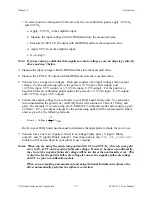
Page 44: ... offset you can determine the offset errors of the DMM by shorting its leads together and reading the measured value This value the DMM offset must be subtracted from all subsequent measurements Gain and Offset Calibration To determine the offset and gain calibration factors of the SCXI 1122 at a given gain Gs perform the following steps for a two point calibration 1 Set the SCXI 1122 to the desir...

Page 45: ... Convert the output voltage from volt units to your DAQ board binary unit You must take into consideration the polarity of your DAQ board its resolution 12 bits or 16 bits and gain For example if you are using an AT MIO 16F 5 in bipolar mode and are using a gain of GMIO 0 5 your output voltages for the autozeroing option will be represented in binary units as given by the following formula Binary ...

Page 46: ... Ω load and measure the voltage 3 Pass this voltage to the SCXI_Cal_Constants function or VI To determine the current excitation calibration constants follow this procedure 1 Set your DMM to DC current measurements 2 Connect the DMM across the IEX and IEX terminals and measure the current 3 Pass this current to the SCXI_Cal_Constants function or VI Note When calibrating your system you must verify...

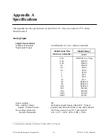
Page 47: ...x Module Range1 Software Selectable 10 V 0 01 250 VDC or Vrms 0 02 250 V 0 05 200 V 0 1 100 V 0 2 50 V 0 5 20 V 1 10 V 2 5 V 5 2 V 10 1 V 20 500 mV 50 200 mV 100 100 mV 200 50 mV 500 20 mV 1 000 10 mV 2 000 5 mV Input coupling DC Max working voltage Each input should remain within 480 Vrms of signal common mode ground and within 250 Vrms of any other channel Overvoltage protection 250 Vrms powered...

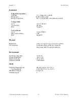
Page 48: ...ndwidth CMRR 50 or 60 Hz 4 Hz 160 dB 4 kHz 100 dB Output range 10 V Output impedance 75 Ω Dynamic Characteristics Bandwidth 3 dB 4 Hz 10 dB or 4 kHz software selectable Settling time to full scale step all gains with 4 kHz filter enabled 10 ms with 4 kHz filter enabled 1 s System noise Gain 4 Hz Filter 4 kHz Filter 1 150 µVrms 1 mVrms 1 000 1 000 nVrms 4 µVrms Slew rate 0 10 V µs Filters Type 3 po...

Page 49: ...pm C Current Mode Level 1 0 mA 0 04 Max load resistance 5 kΩ Drift 40 ppm C Physical Dimensions 3 0 by 17 3 by 20 3 cm 1 2 by 6 8 by 8 0 in I O connectors 50 pin male ribbon cable rear connector 48 pin male DIN C front I O connector Environment Operating temperature 0 to 50 C Storage temperature 20 to 70 C Relative humidity 10 to 90 Maximum altitude 2000 meters Safety Electrical Measuring and IEC ...

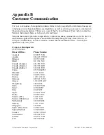
Page 50: ... central time In other countries contact the nearest branch office You may fax questions to us at any time Corporate Headquarters 512 795 8248 Branch Offices Phone Number Australia 03 9879 5166 Austria 0662 45 79 90 0 Belgium 02 757 00 20 Brazil 011 284 5011 Canada Calgary 403 274 9391 Canada Ontario 905 785 0085 Canada Québec 514 694 8521 China 0755 3904939 Denmark 45 76 26 00 Finland 90 725 725 ...

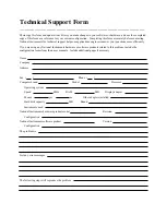
Page 51: ...ficiently If you are using any National Instruments hardware or software products related to this problem include the configuration forms from their user manuals Include additional pages if necessary Name Company Address Fax Phone Computer brand Model Processor Operating system Speed MHz RAM MB Display adapter Mouse yes no Other adapters installed Hard disk capacity MB Brand Instruments used Natio...

Page 52: ...22 Revision Letter _____________________________________________________ Chassis Slot _____________________________________________________ Grounding Shielding and Reference Mode Selection Factory Setting Parking position W1 A R0R1 _____________________________________________________ SERDATOUT Resistor Pull up Jumper Factory Setting Enabled W2 position 1 __________________________________________...
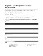
Page 53: ...rogrammer manual Check all that apply National Instruments does not support your operating system or programming language You are an experienced register level programmer who is more comfortable writing your own register level software Other Please explain Thank you for your help Name Title Company Shipping Address Street Address Not P O Box Phone Mail to Customer Service Department Fax to Custome...

Page 54: ...eptember 1999 Part Number 320516B 01 Please comment on the completeness clarity and organization of the manual If you find errors in the manual please record the page numbers and describe the errors Thank you for your help Name Title Company Address Phone Mail to Technical Publications Fax to Technical Publications National Instruments Corporation National Instruments Corporation 11500 N Mopac Exp...

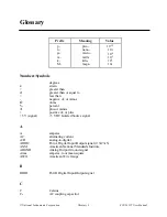
Page 55: ...al to less than negative of or minus Ω ohms percent plus or minus positive of or plus 5 V signal 5 VDC Isolated Source signal A A amperes AC alternating current A D analog to digital ADIO Port A Digital Input Output signal 0 5 ANSI American National Standards Institute AOGND Analog Output Ground signal Arms amperes root mean square AWG American Wire Gauge B BDIO Port B Digital Input Output signal ...

Page 56: ...log DAQD A Data Acquisition Board Data Address Line signal dB decibels DC direct current DIGGND Digital Ground signal DIN Deutsche Industrie Norme DOUT Data Out Number signal E EEPROM electrically erased programmable read only memory F F Farads FSR full scale range G GF gauge factor GMIO MIO gain Gs SCXI gain Gtotal total gain H Hz hertz I Ibias bias current IEX current excitation channel IEX Nega...

Page 57: ...n signal N NMR normal mode rejection NRSE nonreferenced single ended input O OUTREF Output Reference signal P ppm parts per million R R resistor RAM random access memory Rb bias resistor Rbias bias resistor RC resistor capacitor filter Rg strain gauge nominal resistance RSCAL shunt resistor RSE referenced single ended input RSVD Reserved bit signal RTD resistance temperature detector RTSI Real Tim...

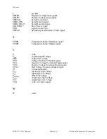
Page 58: ...face Clock signal T TEMP Temperature Sensor Reference signal TEMP Temperature Sensor Output signal V V volts Vcm common mode voltage VDC volts direct current VEX Voltage Excitation Channel signal VEX Negative Voltage Excitation Output signal VEX Positive Voltage Excitation Output signal VEX 2 Half Voltage Excitation Output signal VI Virtual Instrument VIH input logic high voltage VIL input logic l...

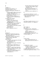
Page 59: ...al 3 11 C cables custom cables 1 5 optional equipment table 1 4 calibration equipment requirements 5 1 to 5 2 excitation calibration 4 4 5 4 gain and offset calibration 5 2 to 5 3 overview 5 1 CH 0 15 signal 3 4 CH 0 15 signal 3 4 configuration See also installation analog configuration 2 3 to 2 5 current loop receivers 2 4 to 2 5 digital signal connections 2 3 jumper settings analog configuration...

Page 60: ...ration 3 7 analog input channel signal connections 3 5 to 3 8 avoiding relay wear illustration 3 8 excitation channel signal connections 3 8 to 3 9 floating AC coupled signal connection referenced to chassis ground for better SNR illustration 3 6 floating signal connection referenced to chassis ground for better SNR illustration 3 6 ground referenced signal connection with high common mode voltage...

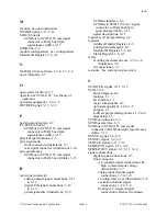
Page 61: ...erface 4 3 SCXIbus to SCXI 1122 rear signal connector to DAQ board pin equivalences table 3 13 signal descriptions 3 11 register level programming 1 4 registers Address Handler Register 4 3 Configuration Register 4 3 Module ID Register 2 3 4 3 Status Register 2 3 4 3 relays avoiding mechanical wear 3 7 to 3 8 illustration 3 8 life expectancy 3 7 resistors See current loop receivers S SCANCLK signa...

Page 62: ...nal 3 11 3 12 software programming choices LabVIEW applications software 1 2 LabWindows applications software 1 2 NI DAQ driver software 1 2 to 1 3 register level programming 1 4 specifications analog input A 1 to A 3 environment A 3 excitation A 3 physical A 3 Status Register 2 3 4 3 T TEMP signal 3 4 3 5 TEMP signal 3 4 3 5 temperature sensor connection 3 9 4 4 theory of operation analog circuit...

Reviews: