background image

© National Instruments

|

2-9

NI PXIe-4300 User Manual

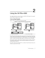
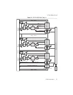
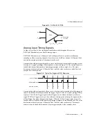
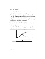
Figure 2-3.  

NI PXIe-4300 PGIA

Analog Input Timing Signals

In order to provide all of the timing functionality described throughout this section, 
NI PXIe-4300 modules have a flexible timing engine.

NI PXIe-4300 modules use AI Sample Clock (ai/SampleClock) to perform simultaneous 
sampling on all active analog channels. Since there is one ADC per channel, AI Sample Clock 
controls the sample period on all the channels in the task.

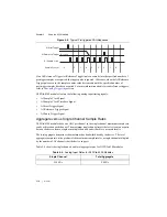
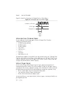
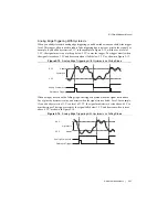
An acquisition with posttrigger data allows you to view data that is acquired after a trigger event 
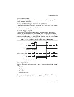
is received. A typical posttrigger DAQ sequence is shown in Figure 2-4. The sample counter is 
loaded with the specified number of posttrigger samples, in this example, five. The value 
decrements with each pulse on AI Sample Clock, until the value reaches zero and all desired 
samples have been acquired.

Figure 2-4.  

Typical Posttriggered DAQ Sequence

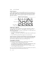
An acquisition with pretrigger data allows you to view data that is acquired before the trigger of 
interest, in addition to data acquired after the trigger. Figure 2-5 shows a typical pretrigger DAQ 
sequence. The AI Start Trigger signal (ai/StartTrigger) can be either a hardware or software 
signal. If AI Start Trigger is set up to be a software start trigger, an output pulse appears on the 
ai/StartTrigger line when the acquisition begins. When the AI Start Trigger pulse occurs, the 
sample counter is loaded with the number of pretrigger samples, in this example, four. The value 
decrements with each pulse on AI Sample Clock, until the value reaches zero. The sample 
counter is then loaded with the number of posttrigger samples, in this example, three.

V

in+

V

m

 = [V

in+

 – V

in–

× 

G

a

in

V

m

V

in–

PGIA

+

Me

asu

red

Volt

a

ge

1

3

0

4

2

AI Start Trigger

AI Sample Clock

Sample Counter

Summary of Contents for NI PXIe-4300

Page 1: ...SC Express NI PXIe 4300 User Manual 8 Ch 250 kS s 300 V Ch Ch Isolated Analog Input Module NI PXIe 4300 User Manual July 2015 373024B 01 ...

Page 2: ...s email addresses and current events National Instruments Corporate Headquarters 11500 North Mopac Expressway Austin Texas 78759 3504 USA Tel 512 683 0100 For further support information refer to the NI Services appendix To comment on National Instruments documentation refer to the National Instruments website at ni com info and enter the Info Code feedback 2010 2015 National Instruments All right...

Page 3: ...ESS FOR A PARTICULAR PURPOSE TITLE OR NON INFRINGEMENT AND ANY WARRANTIES THAT MAY ARISE FROM USAGE OF TRADE OR COURSE OF DEALING NI DOES NOT WARRANT GUARANTEE OR MAKE ANY REPRESENTATIONS REGARDING THE USE OF OR THE RESULTS OF THE USE OF THE PRODUCTS IN TERMS OF CORRECTNESS ACCURACY RELIABILITY OR OTHERWISE NI DOES NOT WARRANT THAT THE OPERATION OF THE PRODUCTS WILL BE UNINTERRUPTED OR ERROR FREE ...

Page 4: ...eir respective companies Patents For patents covering National Instruments products technology refer to the appropriate location Help Patents in your software the patents txt file on your media or the National Instruments Patent Notice at ni com patents Export Compliance Information Refer to the Export Compliance Information at ni com legal export compliance for the National Instruments global tra...

Page 5: ...are Timed Acquisitions 2 7 Hardware Timed Acquisitions 2 7 Analog Input Filter 2 8 Gain 2 8 Analog Input Timing Signals 2 9 Aggregate versus Single Channel Sample Rates 2 10 AI Sample Clock Signal 2 11 AI Sample Clock Timebase Signal 2 12 AI Start Trigger Signal 2 12 AI Reference Trigger Signal 2 14 AI Pause Trigger Signal 2 15 Getting Started with AI Applications in Software 2 16 External Referen...

Page 6: ...2 Figure 2 7 Retriggerable Analog Input 2 13 Figure 2 8 Reference Trigger Final Buffer 2 14 Figure 2 9 Halt Internal Clock and Free Running External Clock 2 15 Figure 2 10 External Clock Reference 2 17 Figure 2 11 Synchronization Operation 2 19 Figure 2 12 Analog Trigger Level 2 20 Figure 2 13 Analog Edge Triggering with Hysteresis on Rising Slope 2 21 Figure 2 14 Analog Edge Triggering with Hyste...

Page 7: ...inal Block Specifications for step by step software and hardware installation instructions Module Specifications Refer to the NI PXIe 4300 Device Specifications document for module specifications Module Accessories and Cables Refer to the NI PXIe 4300 and TB 4300 B C User Guide and Terminal Block Specifications for information about supported accessories and cables Module Self Calibration Self cal...

Page 8: ...aces your module 3 Initiate self calibration using one of the following methods Click Self Calibrate in the upper right corner of MAX Right click the name of the module in the MAX configuration tree and select Self Calibrate from the drop down menu Note You can also programmatically self calibrate the module with NI DAQmx as described in Device Calibration in the NI DAQmx Help or the LabVIEW Help ...

Page 9: ...to the negative terminal of the source as shown in Figure 2 1 or to an isolated ground of the source as long as the working voltage specification of the NI PXIe 4300 is not violated For best results wire the AI and AI signals as twisted pairs and use the COM as a shield The COM connection should be made as close to the source as possible to take advantage of the differential nature of this device ...

Page 10: ...ows the pinout of the front connector of the NI PXIe 4300 Refer to the I O Connector Signal Description section for definitions of each signal Refer to the NI PXIe 4300 and TB 4300 B C User Guide and Terminal Block Specifications for signal locations on the terminal block ...

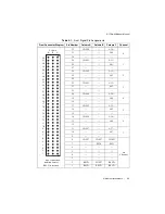
Page 11: ...erved 32 COM 0 AI 0 0 31 AI 0 30 29 COM 1 AI 1 1 28 AI 1 27 26 COM 2 AI 2 2 25 AI 2 24 23 COM 3 AI 3 3 22 AI 3 21 20 COM 4 AI 4 4 19 AI 4 18 17 COM 5 AI 5 5 16 AI 5 15 14 COM 6 AI 6 6 13 AI 6 12 11 COM 7 AI 7 7 10 AI 7 9 8 COM 7 COM 7 COM 7 No Channel 7 PFI 0 PFI 1 6 5 4 3 2 RSVD COM 7 RSVD 1 RSVD RSVD RSVD Column A B C 32 31 30 29 28 27 26 25 24 23 22 21 20 19 18 17 16 15 14 13 12 11 10 9 8 7 6 5...

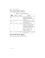
Page 12: ...r differential analog input measurements AI 0 7 AI 0 7 COM 0 7 Input Analog Input Channels 0 to 7 AI and AI are the positive and negative inputs of differential analog input PFI 0 1 COM 7 Input Programmable Function Interface Channels 0 to 1 Each of these terminals can be individually configured as PFI terminals They can be used to supply a start reference or pause trigger or be used as an externa...

Page 13: ...n Isolated Digital Communication PXIe Bus PWM Gain Filter Selection ADC Control Selectable Filter ADC AI CH 0 300 Vrms Isolation AI0 AI0 COM AI7 AI7 COM 96 Pin DIN AI CH 7 300 Vrms Isolation Power Channel Power M CAL MUX PGIA Selectable Filter ADC AI CH 6 AI6 AI6 COM Power Channel Power Power Channel Power Terminal Block Power Isolator Isolator Isolator 300 Vrms Isolation Isolator ...

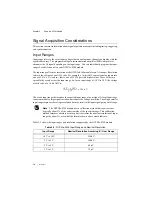
Page 14: ...e spread fairly evenly across the input range So for an input range of 10 V to 10 V the voltage of each code of a 16 bit ADC is Choose an input range that matches the expected input range of your signal A large input range can accommodate a large signal variation but reduces the voltage resolution Choosing a smaller input range improves the voltage resolution but may result in the input signal goi...

Page 15: ... sample of data Hardware Timed Acquisitions With hardware timed acquisitions a digital hardware signal AI Sample Clock controls the rate of the acquisition This signal can be generated internally on your device or provided externally Hardware timed acquisitions have several advantages over software timed acquisitions The time between samples can be much shorter The timing between samples is determ...

Page 16: ...al time control applications HWTSP operations in conjunction with the wait for next sample clock function provide tight synchronization between the software layer and the hardware layer Refer to the whitepaper NI DAQmx Hardware Timed Single Point Lateness Checking for more information To access this document go to ni com info and enter the Info Code daqhwtsp Analog Input Filter The NI PXIe 4300 ha...

Page 17: ... AI Sample Clock until the value reaches zero and all desired samples have been acquired Figure 2 4 Typical Posttriggered DAQ Sequence An acquisition with pretrigger data allows you to view data that is acquired before the trigger of interest in addition to data acquired after the trigger Figure 2 5 shows a typical pretrigger DAQ sequence The AI Start Trigger signal ai StartTrigger can be either a...

Page 18: ...Signal AI Pause Trigger Signal Aggregate versus Single Channel Sample Rates NI PXIe 4300 modules have one ADC per channel so the single channel maximum sample rate can be achieved on each channel The maximum single channel rate is the fastest you can acquire data on the device from a single or multiple channels and still achieve accurate results The total aggregate determines the maximum bus bandw...

Page 19: ... for more information Using an External Source Use one of the following external signals as the source of AI Sample Clock PFI 0 1 PXI_Trig 0 7 PXI_STAR PXIe_DSTAR A B Routing AI Sample Clock Signal to an Output Terminal You can route AI Sample Clock out to any PXI_Trig 0 7 or PXIe_DSTARC terminal This pulse is always active high All PFI terminals are configured as inputs by default Other Timing Re...

Page 20: ...AI Sample Clock Timebase as either rising or falling edge except on 100 MHz Timebase or 20 MHz Timebase AI Start Trigger Signal Use the AI Start Trigger ai StartTrigger signal to begin a measurement acquisition A measurement acquisition consists of one or more samples If you do not use triggers begin a measurement with a software command by starting a task which sends the software command that beg...

Page 21: ...Using a Digital Source To use AI Start Trigger with a digital source specify a source and an edge The source can be any of the following signals PFI 0 1 PXI_Trig 0 7 PXI_STAR PXIe_DSTAR A B The source also can be one of several other internal signals on your DAQ device Refer to Device Routing in MAX in the NI DAQmx Help or the LabVIEW Help for more information You also can specify whether the meas...

Page 22: ...n the buffer to make space for the next sample This data can be accessed with some limitations before the DAQ device discards it Refer to the KnowledgeBase document Can a Pretriggered Acquisition be Continuous for more information To access this KnowledgeBase go to ni com info and enter the Info Code rdcanq When the reference trigger occurs the DAQ device continues to write samples to the buffer u...

Page 23: ...n the signal is inactive You can program the active level of the pause trigger to be high or low as shown in Figure 2 9 In the figure T represents the period and A represents the unknown time between the clock pulse and the posttrigger Figure 2 9 Halt Internal Clock and Free Running External Clock Using a Digital Source To use AI Pause Trigger specify a source and a polarity The source can be any ...

Page 24: ... mechanisms Some of the applications also use start and reference pause triggers Note For more information about programming analog input applications and triggers in software refer to the NI DAQmx Help or the LabVIEW Help in version 8 0 or later NI PXIe 4300 modules use the NI DAQmx driver NI DAQmx includes a collection of programming examples to help you get started developing an application You...

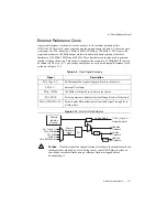
Page 25: ...n Figure 2 10 Figure 2 10 External Clock Reference Caution Do not disconnect an external reference clock once the modules have been synchronized or are used by a task Doing so may cause NI DAQmx to return an error Make sure that all tasks using a reference clock are stopped before disconnecting it Table 2 5 Clock Signal Sourcing Signal Description PXI_Trig 0 7 Bi Directional bus connecting each bo...

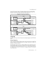
Page 26: ...iple modules depending on your application To synchronize multiple modules to a common timebase choose one module the master to generate the timebase The master module routes its 10 MHz reference clock to one of the PXI_Trig 0 7 signals All modules including the master module receive the 10 MHz reference clock from PXI_Trig This signal becomes the external reference clock A PLL on each module gene...

Page 27: ...ition capabilities The analog trigger signal can be used as a reference trigger only This restriction is due to the fact that the analog trigger circuit operates on digitized ADC data requiring the acquisition to be running in order for the analog trigger circuit to operate In a reference triggered acquisition you configure the device to acquire a certain number of pre trigger samples and a certai...

Page 28: ...hen the sample rate is only twice the bandwidth of interest This jitter usually has no effect on data processing and you can decrease this jitter by sampling at a higher rate Sampling at a rate less than twice the bandwidth of interest may cause the trigger signal to not reliably be detected You can use the following analog triggering modes with the NI PXIe 4300 modules rising edge rising edge wit...

Page 29: ... falls below 2 2 V as shown in Figure 2 13 Figure 2 13 Analog Edge Triggering with Hysteresis on Rising Slope When using hysteresis with a falling slope the trigger is armed when the signal starts above Level plus the hysteresis value and asserts when the signal crosses below Level For example if you add a hysteresis of 1 V to a level of 3 2 V the signal must start at or rise above 4 2 V to arm th...

Page 30: ...fied around the trigger Pause Acquisition is put on hold when trigger is met level sensitive only In addition the trigger circuit provides a programmable filter to help with noisy trigger signals The filter checks that the trigger condition is met for different time intervals before triggering The filter can select from 90 ns 5 12 μs 2 56 ms or a custom defined time interval For information about ...

Page 31: ...t connected accessories in your application Refer to the NI DAQmx Help for documentation about programmatically accessing accessory status Select Start All Programs National Instruments NI DAQmx NI DAQmx Help Accessory Power The NI PXIe 4300 provides auxiliary power for accessories connected to the module and has protection in the event of a fault condition If a fault occurs in the form of an over...

Page 32: ...ndependently to each peripheral slot in a PXI Express chassis For more information refer to the PXI Express Specification at www pxisa org PXI_CLK10 PXI_CLK10 is a common low skew 10 MHz reference clock for synchronization of multiple modules in a PXI measurement or control system The PXI backplane is responsible for generating PXI_CLK10 independently to each peripheral slot in a PXI chassis Note ...

Page 33: ... each PFI PXI_Trig PXIe_DSTAR or PXI_STAR signal PXIe_DSTAR A C PXI Express devices can provide high quality and high frequency point to point connections between each slot and a system timing slot These connections come in the form of three low voltage differential star triggers that create point to point high frequency connections between a PXI Express system timing module and a peripheral devic...

Page 34: ...MA the fastest available data transfer method NI uses DMA hardware and software technology to achieve high throughput rates and increase system utilization DMA is the default method of data transfer for PCI Express and PXI Express devices Programmed I O Programmed I O is a data transfer mechanism where the user s program is responsible for transferring data Each read or write call in the program i...

Page 35: ...s you identify your systems accuracy and reliability requirements and provides warranty sparing and calibration services to help you maintain accuracy and minimize downtime over the life of your system Visit ni com services for more information Warranty and Repair All NI hardware features a one year standard warranty that is extendable up to five years NI offers repair services performed in a time...

Page 36: ...ations Engineers make sure every question submitted online receives an answer Software Support Service Membership The Standard Service Program SSP is a renewable one year subscription included with almost every NI software product including NI Developer Suite This program entitles members to direct access to NI Applications Engineers through phone and email for one to one technical support as well...

Reviews: