


Chapter 3
Hardware Overview
©
National Instruments Corporation
3-3
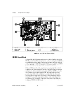
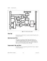
8-Bit ADC and LUT
An 8-bit flash ADC digitizes the image, which is passed to a 256-by-8 bit
lookup table (LUT) RAM. You can configure the input LUT to implement
simple imaging operations such as contrast enhancement, data inversion,
gamma manipulation, or other nonlinear transfer functions.
CSYNC Mux
The composite synchronization (CSYNC) multiplexer lets the genlock
and synchronization circuitry select the internally generated composite
synchronization signal or the composite synchronization signal received
from the I/O connector.
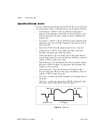
Genlock and Synchronization Circuitry
The genlock and synchronization circuitry receives the incoming video
signal and generates a PCLK, HSYNC, and VSYNC signal for use by the
acquisition and control circuitry. The synchronization circuitry interacts
with the voltage-controlled oscillator (VCO) and phase-locked loop (PLL)
circuitry, which generates and controls the PCLK.
VCO and PLL Circuitry
The VCO and PLL circuitry controls the internally generated PCLK signal
frequency. The 1408 device can digitize an incoming video signal at rates
of up to 16.4 MHz.
Pixel Aspect Ratio Circuitry
The pixel aspect ratio circuitry adjusts the ratio between the physical
horizontal size and the vertical size of the region covered by the pixel.
This value is used to figure the picture aspect ratio. For more information,
see the
section later in this chapter.
PCLK, HSYNC, VSYNC Mux
The acquisition control circuitry selects the clock and synchronization
signals through the pixel clock (PCLK), horizontal synchronization
(HSYNC), and vertical synchronization (VSYNC) multiplexer. The
onboard genlock and synchronization circuitry can generate clock and
synchronization signals or the signals can be received from the I/O
connector.