Chapter 9
Bus Interface
DAQ-STC Technical Reference Manual
9-8
©
National Instruments Corporation
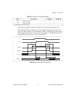
Figure 9-4.
Motorola Bus Interface Write Timing
The DAQ-STC generates an internal read or write signal based upon the read/write, data
strobe, and chip-select signals at the pins. The internal signals will be asserted only when both
the chip-select and data-strobe signals are asserted, shown above as CS-DS. The timing
parameters are all relative to the combined signal.
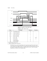
Table 9-3.
Intel Bus Interface Timing
Name
Description
Minimum
Maximum
Tcs-ds
CS-DS pulsewidth
50
—
Tads
Address setup time
0
—
Tadh
Address hold time
6
—
Trws
Rd/wr setup time
3
—
Trwh
Rd/wr hold time
3
—
Tdv
Data valid
13
(50)*
Tdi
Data invalid
4
10
Tds
Data setup time
25
—
Tdh
Data hold time
0
—
All timing values are in nanoseconds.
* Number in parentheses indicates a 100 pF load.
D<0..15>
A<1..7>
CS-DS
DS
RD/WR
CS
Tads
Trws
Trwh
Tds
Tadh
Tdh
Tcs-ds

