

DESIGN CONSIDERATIONS
12
MultiConnect
®
PCIe MTPCIE-EV3 Developer Guide
Chapter 3 – Design Considerations
Design Consideration
When using the Multi-Tech MiniPCIe form factor:
Consult your modem’s device guide for device dimensions. With the modem, the Multi-Tech Mini PCIe form
factor exceeds the standard Mini PCIe maximum component height for top and bottom.
If you need to install components under the module, use taller connectors to avoid conflict. Multi-Tech
recommends not installing components under the module.
Check the
Pinout
table for pins that differ from the MiniPCIe spec.
Noise Suppression Design
Adhere to engineering noise-suppression practices when designing a printed circuit board (PCB). Noise suppression
is essential to the proper operation and performance of the modem and surrounding equipment.
Any OEM board design must consider both on-board and off-board generated noise that can affect digital signal
processing. Both on-board and off-board generated noise that is coupled on-board can affect interface signal levels
and quality. Noise in frequency ranges that affect modem performance is of particular concern.
On-board generated electromagnetic interference (EMI) noise that can be radiated or conducted off-board is
equally important. This type of noise can affect the operation of surrounding equipment. Most local government
agencies have certification requirements that must be met for use in specific environments.
Proper PC board layout (component placement, signal routing, trace thickness and geometry, and so on)
component selection (composition, value, and tolerance), interface connections, and shielding are required for the
board design to achieve desired modem performance and to attain EMI certification.
Other aspects of proper noise-suppression engineering practices are beyond the scope of this guide. Consult noise
suppression techniques described in technical publications and journals, electronics and electrical engineering text
books, and component supplier application notes.
PC Board Layout Guideline
In a 4-layer design, provide adequate ground plane covering the entire board. In 4-layer designs, power and ground
are typically on the inner layers. Ensure that all power and ground traces are 0.05 inches wide.
Electromagnetic Interference
The following guidelines are offered specifically to help minimize EMI generation. Some of these guidelines are the
same as, or similar to, the general guidelines. To minimize the contribution of device-based design to EMI, you
must understand the major sources of EMI and how to reduce them to acceptable levels.
Keep traces carrying high frequency signals as short as possible.
Provide a good ground plane or grid. In some cases, a multilayer board may be required with full layers for
ground and power distribution.
Decouple power from ground with decoupling capacitors as close to the device's power pins as possible.
Eliminate ground loops, which are unexpected current return paths to the power source and ground.
Summary of Contents for MultiConnect MTPCIE-EV3
Page 1: ...MultiConnect PCIe MTPCIE EV3 Developer Guide ...
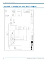
Page 15: ...DEVELOPER BOARD MultiConnect PCIe MTPCIE EV3 Developer Guide 15 ...
Page 17: ...ASSEMBLY DIAGRAM MultiConnect PCIe MTPCIE EV3 Developer Guide 17 Bottom ...
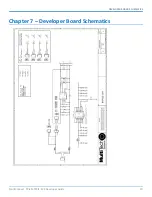
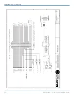
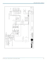
Page 20: ...DEVELOPER BOARD SCHEMATICS 20 MultiConnect PCIe MTPCIE EV3 Developer Guide ...
Page 21: ...DEVELOPER BOARD SCHEMATICS MultiConnect PCIe MTPCIE EV3 Developer Guide 21 ...
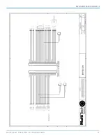
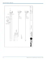
Page 22: ...DEVELOPER BOARD SCHEMATICS 22 MultiConnect PCIe MTPCIE EV3 Developer Guide ...
Page 23: ...DEVELOPER BOARD SCHEMATICS MultiConnect PCIe MTPCIE EV3 Developer Guide 23 ...
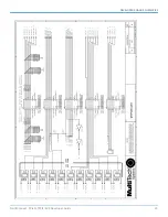
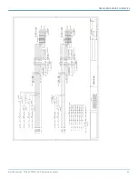
Page 24: ...DEVELOPER BOARD SCHEMATICS 24 MultiConnect PCIe MTPCIE EV3 Developer Guide ...
Page 25: ...DEVELOPER BOARD SCHEMATICS MultiConnect PCIe MTPCIE EV3 Developer Guide 25 ...
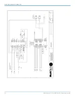
Page 26: ...DEVELOPER BOARD SCHEMATICS 26 MultiConnect PCIe MTPCIE EV3 Developer Guide ...
Page 27: ...DEVELOPER BOARD SCHEMATICS MultiConnect PCIe MTPCIE EV3 Developer Guide 27 ...