3-22
BIOS Setup
▍
MS-7589
BIOS Setup
▍
MS-7589
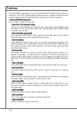
“Advance DRAM Configuraton” sub-menu to be determned by BIOS based on the con-
figuratons on the SPD. Selectng [Manual] allows users to configure the DRAM tmngs
and the followng related “Advance DRAM Configuraton” sub-menu manually.
Advance DRAM Configuraton
Press <Enter> to enter the sub-menu.
CH1/ CH2 1T/2T Memory Tmng
Ths tem controls the SDRAM command rate. Select [1N] makes SDRAM sgnal
controller to run at 1N (N=clock cycles) rate. Selectng [2N] makes SDRAM sgnal
controller run at 2N rate.
CH1/ CH2 CAS Latency (CL)
Ths controls the CAS latency, whch determnes the tmng delay (n clock cycles)
before SDRAM starts a read command after recevng t.
CH1/ CH2 tRCD
When DRAM s refreshed, both rows and columns are addressed separately. Ths
setup tem allows you to determne the tmng of the transton from RAS (row ad-
dress strobe) to CAS (column address strobe). The less the clock cycles, the faster
the DRAM performance.
CH1/ CH2 tRP
Ths settng controls the number of cycles for Row Address Strobe (RAS) to be
allowed to precharge. If nsufficent tme s allowed for the RAS to accumulate ts
charge before DRAM refresh, refresh may be ncomplete and DRAM may fal to
retan data. Ths tem apples only when synchronous DRAM s nstalled n the sys-
tem.
CH1/ CH2 tRAS
Ths settng determnes the tme RAS takes to read from and wrte to memory cell.
CH1/ CH2 tRFC
Ths settng determnes the tme RFC takes to read from and wrte to a memory
cell.
CH1/ CH2 tWR
Mnmum tme nterval between end of wrte data burst and the start of a precharge
command. Allows sense amplfiers to restore data to cells.
CH1/ CH2 tWTR
Mnmum tme nterval between the end of wrte data burst and the start of a col-
umn-read command. It allows I/O gatng to overdrve sense amplfiers before read
command starts.
CH1/ CH2 tRRD
Specfies the actve-to-actve delay of dfferent banks.
CH1/ CH2 tRTP
Tme nterval between a read and a precharge command.
CH1/ CH2 tFAW
Ths tem s used to set the tFAW tmng.
▶
▶
▶
▶
▶
▶
▶
▶
▶
▶
▶
▶
Summary of Contents for P55-GD51
Page 1: ... P55 GD55 P55 GD51 series MS 7589 v1 x Mainboard G52 75891X7 ...
Page 10: ......
Page 16: ......
Page 42: ......
Page 122: ......

