44
Chapter 7. Digital I/O
Pin
Signal
Pin
Signal
Pin
Signal
1
3.3 V
11
A4
21
GND
2
3.3 V
12
A5
22
GND
3
3.3 V
13
A6
23
B4
4
GND
14
A7
24
B5
5
A0
15
GND
25
B6
6
A1
16
GND
26
B7
7
A2
17
B0
27
GND
8
A3
18
B1
28
GND
9
GND
19
B2
29
GND
10
GND
20
B3
30
GND
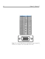
Figure 7.2:
High-speed digital IO connector (internal). Note that the
FFC
cable can be inserted upside-down, reversing the pin ordering.
Version
Driver
Bank size
Example configuration
Rev2
74LVT2244
Outputs only
16x outputs
Rev3-4
74LVTH2245
Banks of 8
8x inputs, 8x outputs
Rev5+
74LVTH162245
Sub-banks of 4
4x inputs, 12x outputs
Table 7.1:
High-speed
I/O
configuration options
Rev5+
hardware can either configure the banks of 8 pins as above,
or
control
sub-banks
of
4
lines.
For
example
to
set
pins
D1-D4
(sub-bank 1A) as inputs and pins D5-D8 (sub-bank 1B) as outputs,
use the command:
EXTIO,MODE,1,HSB,READ,WRITE
Summary of Contents for ARF021
Page 1: ...Agile RF Synthesizer AOM driver ARF021 ARF421 XRF021 XRF421 Version 1 5 0 Rev 6 ...
Page 4: ...ii ...
Page 10: ...viii Contents ...
Page 26: ...16 Chapter 3 Communications ...
Page 44: ...34 Chapter 5 External modulation ...
Page 50: ...40 Chapter 6 PID stabilisation ...
Page 64: ...54 Chapter 7 Digital I O ...
Page 100: ...90 Chapter 9 Advanced table mode XRF ...
Page 128: ...118 Appendix C Command language ...
Page 133: ......

