background image


A - 2                                                                                                                                                  A - 2 

[WIRING PRECAUTIONS] 

!

 CAUTION 

 Ground the AG and FG terminals to the protected grounding conductor when there are a lot of 

noise.  Failure to ground these terminals may cause malfunctions. 

 When wiring PLC, check the rated voltage and terminal layout of the wiring, and make sure the 

wiring is done correctly.  Connecting a power supply that differs from the rated voltage or wiring 
it incorrectly may cause fires or failure. 

 Tighten the terminal screws within the range of specified torque. 

If the terminal screws are loose, it may result in short circuits or malfunctions. 
Tightening the screws too far may cause damage to the screw, resulting in short circuits, or 
malfunctions. 

 Be sure there are no foreign substances such as sawdust or wiring debris inside the module.  

Such debris could cause fires, failure, malfunctions. 


[STARTING AND MAINTENANCE PRECAUTIONS] 

!

 CAUTION 

 Do not touch the connector while the power is on. Doing so could cause malfunctions. 

 Be sure to shut off all phases of the external power supply used by the system before cleaning 

or retightening the terminal screws. If you do not switch off the external power supply, it will 
cause failure or malfunctions of the module. 

 Do not disassemble or modify the modules. Doing so could cause failure, malfunctions, injury, or 

fires. 

 Be sure to shut off all phases of the external power supply used by the system before mounting 

or dismounting the module. If you do not switch off the external power supply, it will cause failure 
or malfunctions of the module. 

 Do not install/remove the terminal block more than 50 times after the first use of the product. 

(IEC 61131-2 compliant) 

 Before handling the module, always touch grounded metal, etc. to discharge static electricity 

from the human body. 
Failure to do so can cause the module to fail or malfunction. 


[OPERATING PRECAUTIONS] 

!

 DANGER 

 Do not output (turn ON) the "usage disable" signal as an output signal to special modules from 

the PLC CPU. 
Outputting the "usage disable" signal may cause PLC system malfunctions. 


[DISPOSAL PRECAUTIONS] 

!

 CAUTION 

 When disposing of this product, treat it as industrial waste. 


Summary of Contents for A1S66ADA

Page 1: ...t Output Module Type A1S66ADA User s Manual Specifications subject to change without notice When exported from Japan this manual does not require application to the Ministry of Economy Trade and Industry for service transaction permission HEAD OFFICE 1 8 12 OFFICE TOWER Z 14F HARUMI CHUO KU 104 6212 JAPAN NAGOYA WORKS 1 14 YADA MINAMI 5 CHOME HIGASHI KU NAGOYA JAPAN ...

Page 2: ......

Page 3: ...ER In case of the external power supply failure or the programmable controller PLC failure set up a safety circuit outside the PLC so that the entire system can operate safely The mis output and malfunction may cause an accident CAUTION Use the PLC in an environment that meets the general specifications contained in this manual Using this PLC in an environment outside the range of the general spec...

Page 4: ...ns Be sure to shut off all phases of the external power supply used by the system before cleaning or retightening the terminal screws If you do not switch off the external power supply it will cause failure or malfunctions of the module Do not disassemble or modify the modules Doing so could cause failure malfunctions injury or fires Be sure to shut off all phases of the external power supply used...

Page 5: ... 66819 F Correction SAFETY PRECAUTIONS Section 4 5 2 June 2005 IB NA 66819 G Addition Conformation to the EMC Directive and Low Voltage Instruction Correction SAFETY PRECAUTIONS Chapter 5 Sep 2006 IB NA 66819 H Correction SAFETY PRECAUTIONS Jul 2007 IB NA 66819 I Correction Section4 4 Section4 5 2 Appendix2 Japanese Manual Version SH 3642 J This manual confers no industrial property rights or any ...

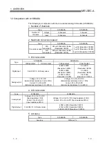
Page 6: ...put characteristic 3 5 3 3 2 Current output characteristic 3 6 3 3 3 Overall accuracy 3 7 3 4 A D Conversion I O Characteristic 3 8 3 4 1 Voltage input characteristic 3 9 3 4 2 Current input characteristic 3 10 3 4 3 Overall accuracy 3 11 3 5 I O Signals Against the PLC CPU 3 12 3 5 1 List of I O signals 3 12 3 5 2 I O signal functions 3 13 4 PROCEDURES AND SETTINGS BEFORE OPERATION 4 1 to 4 12 4 ...

Page 7: ...rent as digital values A D conversion 5 1 5 2 Basic Read and Write Programs 5 2 5 3 Program Example 5 3 6 TROUBLESHOOTING 6 1 to 6 2 APPENDIX App 1 to App 5 Appendix 1 Comparison with the Conventional Analog I O Module A1S63ADA App 1 Appendix 2 External Dimensions App 3 Appendix 3 Precautions For Reading A Digital Output Value For Hardware Version C or Earlier App 4 ...

Page 8: ...fer to Chapter 3 EMC Directives and Low Voltage Directives of the User s Manual Hardware included with the CPU module or base unit used The CE logo is printed on the rating plate on the main body of the PLC that conforms to the EMC directive and low voltage instruction By making this product conform to the EMC directive and low voltage instruction it is not necessary to make those steps individual...

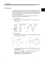
Page 9: ...ital conversion 1 D A conversion Digital values are converted to analog values such as voltage and current and output externally 100 200 400 500 300 100 300 200 V 0 t Digital values Analog values 2 A D Conversion Analog values such as voltage and current are converted to digital values so they can be imported into the PLC CPU V V 0 t t 0 Digital values Analog values The voltage current and digital...

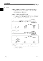
Page 10: ...K1 FROM H0 K1 D1 K1 The digital value to undergo D A conversion is written The digital value that has been undergone A D conversion is read Processing time Item A2USHCPU Q2ASHCPU TO 212 1 μs 162 0 μs Command FROM 183 5 μs 160 0 μs Total 395 6 μs 322 0 μs I O signal X Y format MOV D0 K3Y0 MOV K3X0 D100 The digital value to undergo D A conversion is written The digital value that has been undergone ...

Page 11: ...to 4000 Resolution 1 4000 8000 to 8000 Resolution 1 8000 12000 to 12000 Resolution 1 12000 0 to 4000 Resolution 1 4000 0 to 8000 Resolution 1 8000 0 to 12000 Resolution 1 12000 Analog output Voltage 10 to 10 V DC External load resistance 2 kΩ to 1 MΩ Current 0 to 20 mA DC External load resistance 0 Ω to 600 Ω Voltage 10 to 0 to 10 V DC External load resistance 2 kΩ to 1 MΩ Current 20 to 20 mA DC E...

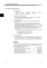
Page 12: ... extension base module and extension cable by taking the following points into consideration 1 Current capacity of the power supply module on the basic base module 2 Voltage drops of the basic base module 3 Voltage drops of the extension base module 4 Voltage drops in the extension cable 4 Data link system In a data link system the module may be loaded to the master station local station or remote...

Page 13: ...2 2 2 2 MELSEC A 2 SYSTEM CONFIGURATION 2 MEMO ...

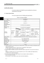
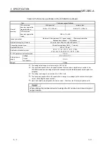
Page 14: ...IS B3502 IEC 61131 2 147 m s 2 3 times each in 3 directions Operating environment No corrosive gas present Operating height 2000 m 6562 ft or less Installation area On the control board Over voltage category 1 II or less Pollution rate 2 2 or less 1 Indicates the distribution area where the device is assumed to be connected from the public power distribution network to the local machine device Cat...

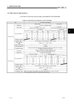
Page 15: ...rent 28 mA Output short protection Present Analog output points 2 channels D A conversion Offset gain adjustment Adjust the two channels simultaneously with the control knob on the front side of the module The adjustment should be done on line Analog input Voltage 10 to 0 to 10 V DC Input resistance 1 MΩ Current 0 to 20 mA DC Input resistance 250 Ω Digital output 0 to 4095 12 bit binary value Anal...

Page 16: ...3 1 25 YS3 2 3 5 2 YS3A V1 25 M3 V1 25 YS3A V2 S3 V2 YS3A 5 V DC internal current consumption 0 21 A Voltage 21 6 to 26 4 V DC External power supply Current consumption 0 16 A Weight 0 33 kg 1 The analog output range is set commonly for CH1 to CH2 2 The conversion speed refers to the speed between the times when a digital value is written to the A1S66ADA and when an analog output which corresponds...

Page 17: ...e current value or voltage value that is output from the A1S66ADA when the digital value set by the PLC CPU is 0 b Gain value The current value or voltage value that is output from the A1S66ADA when the digital value set by the PLC CPU is 4000 3 I O conversion characteristic Examples of A1S66ADA s I O conversion characteristic are shown below V 10 5 0 5 10 Offset value Gain value 0 2000 4000 When ...

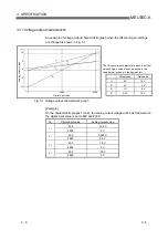
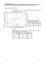
Page 18: ...w is shown in the figure at left Offset value Gain value 1 0 V 10 V 2 0 V 5 V 3 1 V 5 V 4 10 V 10 V 5 0 5 10 10 V 0 2000 4000 Digital input value Analog output voltage 4 2 3 1 Fig 3 1 Voltage output characteristic graph Example On the characteristic graphs 1 to 4 the analog output voltage will be as follows when the digital input value is set to 500 and 2000 No Digital input value Analog output va...

Page 19: ...set as shown in the table below is shown in the figure at left Offset value Gain value 1 0 mA 20 mA 2 4 mA 20 mA 15 10 5 0 20 m A 0 2000 4000 Digital input value Analog output current 1 2 Fig 3 2 Current output characteristic graph Example On the characteristic graphs 1 to 2 the analog output voltage will be as follows when the digital input value is set to 1000 and 2000 No Digital input value Ana...

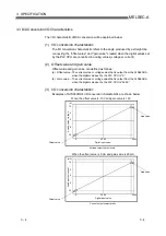
Page 20: ...own in Fig 3 3 and 3 4 10V 0V 10V 0 2000 4000 Analog output value Digital input value Fluctuation will be within 10 V 1 100 mV width due to the operating environment ambient temperature noise The overall accuracy of the voltage output is the accuracy against 10V Fig 3 3 Overall accuracy of voltage output characteristics 20mA 0mA 0 4000 Analog output value Digital input value Fluctuation will be wi...

Page 21: ...LC CPU are converted to analog values voltage or current 2 Offset value and gain value Offset value and gain value are defined as follows a Offset value The analog value voltage or current that makes the digital output value 0 b Gain value The analog value voltage or current that makes the digital output value 4000 3 I O conversion characteristic Examples of A1S66ADA s I O conversion characteristi...

Page 22: ...output voltage will be as follows when the analog input value is set to 1 V and 3 V No Analog input value Digital output value 1 V 400 1 3 V 1200 1 V 800 2 3 V 2400 1 V 0 3 3 V 2000 1 V 2200 4 3 V 2600 POINT When a voltage that exceeds the range of 15 V to 15 V is input the elements may be damaged The overall accuracy is the accuracy outlined in the performance specifications when the input voltag...

Page 23: ...ital output current will be as follows when the analog input value is set to 5 mA and 12 mA No Analog input value Digital output value 5 mA 1000 1 12 mA 2400 8 mA 250 2 12 mA 2000 POINT When a current exceeding the range of 30mA to 30mA is input the elements may be damaged due to heating The overall accuracy is the accuracy outlined in the performance specifications when the input current is in th...

Page 24: ... as outlined in the specification The overall accuracy of voltage and current input characteristics are shown in Fig 3 7 and 3 8 5 5 15 10 0 10 15 Offset value 0 V gain value 10 V resolution 1 4000 1 40 0 1000 2000 3000 4000 Digital output value Analog input voltage V Fig 3 7 Overall accuracy of voltage input characteristic 0 10 20 2000 4000 4095 0 Analog input current mA Digital output value 1 40...

Page 25: ...rection A1S66ADA PLC CPU Signal Direction PLC CPU A1S66ADA Device No Signal Name Device No Signal Name X00 to X0B CH3 digital output value Y00 to Y0B CH1 digital value setting Y0C to Y0E Usage disable X0C to X0F Usage disable Y0F CH1 D A conversion value output enable flag X10 to X1B CH4 digital output value Y10 to Y1B CH2 digital value setting Y1C to Y1E Usage disable X1C to X1F Usage disable Y1F...

Page 26: ...n6 Xn5 Xn4 Xn3 Xn2 Xn1 Xn0 7 D 0 2 Y00 to Y0B Y10 Y1B Digital value setting The digital values to be D A converted in CH1 and CH2 are set in Yn0 to YnB as binary data as shown below Digital value setting 0 to 4000 b11 b10 b9 b8 b7 b6 b5 b4 b3 b2 b1 b0 YnB YnA Yn9 Yn8 Yn7 Yn6 Yn5 Yn4 Yn3 Yn2 Yn1 Yn0 Example When the digital value in CH2 is set to 2500 H09C4 YnB YnA Yn9 Yn8 Yn7 Yn6 Yn5 Yn4 Yn3 Yn2 Y...

Page 27: ...re the operation of the module are shown in Fig 4 1 below Start Install the A1S66ADA in the appropriate slot Module installation Wiring Create and check programs for reading and writing to the A1SA66ADA from the PC CPU Programming Debugging Offset Gain Settings Set the offset values and gain values for the channels to be used Perform wiring for A1S66ADA and external devices End Refer to Section 4 ...

Page 28: ...4 Tighten the module installation screws and terminal screws within the range as follows Screw Area Tightening Torque Range Module fixing screws M4 screw 78 to 118 N cm Terminal block terminal screws M3 5 screw 59 to 88 N cm Terminal block installation screws M4 screw 78 to 118 N cm 5 When loading the module to the base unit be sure to insert the module latch to the fixing hole and secure the modu...

Page 29: ...odule install the cover to the terminal side first as shown in the figure then it will be completed by pushing the cover to the module and tightening the shield fixing screw 2 Removal Module Shield cover Hole for removal Shield fixing screw To remove the shield cover from the module remove the shield fixing screw first and install the tip of a flat tip screwdriver into the removal hole as shown in...

Page 30: ...tings of the A1S66ADA 0 10V 0 5V 1 5V 10 10V D A A D OFFSET GAIN RUN A D D A A1S66ADA C H 1 C H 2 C H 3 C H 4 C H 5 C H 6 V COM I V V I COM SLD SLD AG FG I V I V I V I V I V I V I V I 24VDC 1 2 3 4 5 6 7 8 9 10 11 13 12 INPUT D A A D 0 10 V 0 20 mA A1S66ADA I N I N O U T V I CH3 CH4 CH5 CH6 1 2 3 4 5 6 7 8 9 10 11 12 13 14 15 16 17 18 19 20 14 ...

Page 31: ...ft 4 A D conversion offset control knob A D OFFSET Used when making a fine adjustment of the A D conversion offset The offset value is increased by turning the control knob to the right The offset value is decreased by turning the control knob to the left 5 A D conversion gain control knob A D GAIN Used when making a fine adjustment of the A D conversion gain The gain value is increased by turning...

Page 32: ...A Jumper When setting to 0 to 10 V When setting to 0 to 20 mA 12 Analog input voltage current switching setting pin V I CH3 CH4 CH5 CH6 Set the analog input voltage input or current input for each channel CH3 to CH6 Set it with the jumper Setting at shipment V For voltage input setting V For current input setting I 13 Analog input range switching setting pin 0 10 V 0 5 V 1 5 V 10 10 V A D Set the ...

Page 33: ...s described below make more improvement in the wiring not to be affected by the noise 1 Use separate cables for the AC and the analog input to the A1S66ADA in order not to be affected by the AC side surge or conductivity 2 Do not bundle or place the cable close to the main circuit line high voltage line or load carrying wires from other than the PLC It is influenced more easily by the noise surge ...

Page 34: ... b For current output GND CH1 or CH2 I COM to 0 600 1 2 D A conversion circuit Motor drive module etc 1 Use a two core twisted shield line for the power cable 2 When noise or ripple occurs with the external cable connect a condenser with 0 1 to 0 47 μ FWV to the input terminal of the external device IMPORTANT The voltage and current output can not be used simultaneously on the same channel In the ...

Page 35: ...istance of 25V or more between the terminal V I and V I 4 The FG terminal of the power supply module should always be grounded 5 Make sure to connect between the FG of the power supply module and the FG of A1S66ADA 6 Due to noise in the environment AG terminal may attain better accuracy when grounded POINT The FG terminal of A1S66ADA and the FG terminal of the power supply module are not connected...

Page 36: ...version to CH3 1 Fine adjustment procedures for the D A conversion offset gain values Start End Set the analog output range by using the analog output range switching setting pin Input the offset value to the output signals Y00 to Y0B Input the gain value to the output signals Y00 to Y0B Adjust the analog output of the CH1 that corresponds to the gain value using D A conversion gain control knob T...

Page 37: ... Adjust the CH3 digital output value X00 to X0B using A D conversion offset control knob so that the value is the same as the offset value Adjust the CH3 digital output value X00 to X0B using A D conversion gain control knob so that the value is the same as the gain value Fine adjustment of the offset value Fine adjustment of the gain value Select the analog input voltage current input with the an...

Page 38: ...TINGS BEFORE OPERATION 4 7 Maintenance and Inspection The A1S66ADA has no particular inspection items but in order to maintain the system in the best condition perform inspection according to the categories listed in the PLC CPU Users Manual ...

Page 39: ... flowcharts 5 1 1 Outputting digital values as voltage current D A conversion The following flow shows the procedure to create a program that converts the digital value input to CH1 and CH2 into analog values voltage current Start Offset gain value setting Initial setting Digital value setting Y00 to Y0B Y10 to Y1B D A conversion value output enable disable setting Y0F Y1F End 5 1 2 Receiving volt...

Page 40: ...hen writing the binary data stored in D10 to I O signals Y40 to Y4B MOV D10 K3Y40 MOV instruction execution condition 2 Read from A1S66ADA MOV MOVP instruction Form MOV P S D MOV P instruction execution condition Symbol Description Usable device S Head number of the I O signals where data is stored X Y D Head number of the device where the data read is to be stored T C D W R Example When assigning...

Page 41: ...y module A 1 S C P U A 1 S 6 6 A D A A 1 S X 4 1 A 1 S Y 4 1 32 points 32 points X Y00 to X Y3F X40 to X5F Y60 to Y7F I O number 2 Initial setting description 1 D A conversion value output enable channel 1 channel 3 Device to be used by user 1 Offset value setting command signal X40 2 Gain value setting command signal X41 3 Digital setting value input command signal X42 4 Digital output value read...

Page 42: ...11 CH 5 digital output value is read to D12 CH 6 digital output value is read to D13 Input X50 to X5F from BCD digital switch is converted to bynary and then stored in D0 Digital setting command Digital read command Digital setting storage Digital setting storage CH 1 digital value setting CH 3 digital output Digital value setting CH 4 digital output CH 5 digital output CH 6 digital output CH 3 an...

Page 43: ...the digital output value by disconnecting the cable for the analog input of the A1S66ADA then applying the test voltage stabilized power supply or batteries to the terminal of the main module Check the grounding method and wiring as it may be influenced by the noise from the external wiring if the digital output values are normal at the individual A1S66ADA station Is the 24VDC power supply turned ...

Page 44: ...6 2 6 2 MELSEC A 6 TROUBLESHOOTING 6 MEMO ...

Page 45: ...fset gain adjustment Adjust using the front knob Perform on line adjustment for the 2 CH in batch Set using the front switch D A conversion No of channels 2 channels 1 channel Analog input Digital output Analog input Digital output 0 to 10 V 4000 to 4000 0 to 5 V 8000 to 8000 1 to 5 V 10 to 10 V 12000 to 12000 10 to 10 V 2000 to 2000 0 to 20 mA 4000 to 4000 I O characteristics 4 to 20 mA 0 to 4000...

Page 46: ...hotocoupler insulation Between channels No insulation Number of I O occupied points 64 points 32 points Connected terminal base 20 points terminal block M3 5 7 screw Applicable wire size 0 75 to 1 25 mm2 Applicable solderless terminal R1 25 3 1 25 YS3 2 3 5 2 YS3A V1 25 M3 V1 25 YS3A V2 S3 V2 YS3A 1 25 3 5 1 25 YS3A 2 3 5 2 YS3A V1 25 M3 V1 25 YS3A V2 S3 V2 YS3A 5 V DC internal current consumption...

Page 47: ...ernal Dimensions 34 5 93 6 130 3 69 1 36 5 12 OFFSET GAIN RUN A D D A A1S66ADA C H 1 C H 2 C H 3 C H 4 C H 5 C H 6 V COM I V V I COM SLD SLD AG FG I V I V I V I V I V I V I V I 24VDC INPUT D A A D 0 10 V 0 20 mA A1S66ADA I N I N O U T Unit mm in ...

Page 48: ...sing Read processing from PLC CPU Read data 0 0000H 256 0100H Digital output value 256 0100H 255 00FFH Lower order byte Xn0 to Xn7 read FFH Higher order byte Xn8 to XnB read 01H Lower order byte Xn0 to Xn7 read 00H Higher order byte Xn8 to XnB read 00H Example 1 When a digital output value is read from the PLC CPU during A D conversion processing during carry occurrence of the A1S66ADA Example 2 W...

Page 49: ...ata register D0 5 Digital output value comparison data storage data register D1 6 D0 D1 difference storage data register D2 7 Normal digital output value storage data register D10 Digital output value comparison source data of Channel 3 is read to D0 Digital output value comparison data is read at next scan and mode shifts to comparison control Digital output value comparison data of Channel 3 is ...

Page 50: ... user 2 Onerous repair term after discontinuation of production 1 Mitsubishi shall accept onerous product repairs for seven 7 years after production of the product is discontinued Discontinuation of production shall be notified with Mitsubishi Technical Bulletins etc 2 Product supply including repair parts is not available after production is discontinued 3 Overseas service Overseas repairs shall ...

Page 51: ......
Page 52: ...ations subject to change without notice When exported from Japan this manual does not require application to the Ministry of Economy Trade and Industry for service transaction permission HEAD OFFICE TOKYO BUILDING 2 7 3 MARUNOUCHI CHIYODA KU TOKYO 100 8310 JAPAN NAGOYA WORKS 1 14 YADA MINAMI 5 CHOME HIGASHI KU NAGOYA JAPAN ...

Reviews: