E a s y M x
P R O
v 7 a
U s e r M a n u a l
P A G E 17
mikroBUS
™
SOCKETS
The superior connectivity features of the EasyMx PRO v7a development board are
rounded up with two standardized mikroBUS
™
host connectors. It is a considerable
upgrade for the board, as it allows interfacing with the vast amount of
Click boards
™
.
mikroBUS
™
is the add-on board standard that offers maximum expandability with
the smallest number of pins. More information at
www.mikroe.com/mikrobus
All the
mikroBUS
™
sockets
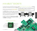
are now redesigned and improved. They became much
sturdier, allowing a better grip of the Click board
™
. In addition to added horizontal
supports between two 8-pin connectors, the right lower edge is chamfered at
the angle of 45°, the same as the Click board
™
, making it seamlessly fit into the
mikroBUS
™
socket. The new mikroBUS
™
socket is now a fully-fledged, standardized
monolithic component with all its pins clearly labeled, offering very good grip for the
Click board
™
, preventing it to flip over or to be placed incorrectly.
The mikroBUS
™
socket supports the following communication interfaces:
SPI, UART
,
and
I
2
C
. There are also single pins reserved for
PWM
,
Interrupt
,
Analog input
,
Reset
,
and
SPI Chip Select
. The mikroBUS
™
socket also contains pins with the two power
rails (
3.3V and 5V
), along with the
GND pins
.
R90
1K
VCC-3.3V
VCC-5V
AN
RST
CS
SCK
MISO
MOSI
3.3V
GND
PWM
INT
RX
TX
SCL
SDA
5V
GND
1
R91
1K
VCC-3.3V
VCC-5V
AN
RST
CS
SCK
MISO
MOSI
3.3V
GND
PWM
INT
RX
TX
SCL
SDA
5V
GND
2
RC5
RC4
RC3
RE1
RE0
RA2
RC6
RC7
RC3
RC4
RC0
RB0
RC5
RC4
RC3
RE2
RA5
RA3
RC6
RC7
RC3
RC4
RC1
RB1
mikroBUS
™
sockets schematic
mikroBUS
™
is not made to be only a part of our development boards. You can
freely place mikroBUS
™
host connectors in your final PCB designs, as long as
you clearly mark them with mikroBUS
™
logo and footprint specifications. For
more information, logo artwork and PCB files visit our website:
www.mikroe.com/mikrobus
Integrate mikroBUS
™
in your design
mikroBUS™ SOCKET IN DETAIL
Analog pin –
AN
Reset pin –
RST
SPI Chip Select line –
CS
SPI Clock line –
SCK
SPI Slave Output line –
MISO
SPI Slave Input line –
MOSI
VCC-3.3V power line –
+3.3V
Reference Ground –
GND
PWM
- PWM output line
INT
- Hardware Interrupt line
RX
- UART Receive line
TX
- UART Transmit line
SCL
- I2C Clock line
SDA
- I2C Data line
+5V
- VCC-5V power line
GND
- Reference Ground
CONNECTIVITY
P A G E 17


