background image

SA.45s Chip-Scale Atomic Clock

SA.45s CSAC User Guide Revision D

7

1.  

2.  

R. Lutwak, et. al., The Chip-Scale Atomic Clock - Low-Power Physics Package, Proceedings of the 36th 
Annual Precise Time and Time Interval (PTTI) Systems and Applications Meeting, December 7–9, 
2004, Washington, DC.
R. Lutwak, et. al., The MAC - A Miniature Atomic Clock, Proceedings of the 2005 Joint IEEE 
International Frequency Control Symposium and Precise Time & Time Interval Systems & 
Applications Meeting, August 29–31, 2005, Vancouver, BC.

3.3.2

Start-Up Sequence

Caution: To avoid severe damage to the unit, do not apply power to the incorrect terminals. The SA.45s 
does not have reverse voltage protection.

When power is connected to pin 7, the SA.45s unit begins its warm-up cycle. A signal appears at the 
output once power is applied to the unit. This output signal is not stable until the oscillator is locked 
(indicated by the BITE pin at CMOS_low).

After 3 minutes, the CSAC achieves Lock and BITE = 0 (

). 

"Built-In Test Equipment (BITE)" (see page 7)

Power consumption during warm-up is greater than during normal operation; it is specified on the 

CSAC 

.

datasheet

It is recommended to always allow CSAC to remain powered on for >102 seconds after it acquires LOCK. 
102 seconds is the minimum amount of time necessary to save CSAC set points to memory. Otherwise, 
upon the next power up, the unit may go in to a mode of operation where it re-acquires all of its set 
points; warm-up time will then be out of specification.

3.3.3

Built-In Test Equipment (BITE)

CSAC state-of-health can be monitored electronically on pin 4 (BITE) of the SA.45s CSAC. Frequency lock 
is indicated both by status = 0 in the status field of telemetry and by the electrical state of the BITE 
output pin, which is high (logic 1) upon initial power-on and whenever status ≠ 0. The BITE pin is a high- 
impedance CMOS logic output.

Note: When not locked, BITE = 1 and also status ≠ 0 in the status field of the telemetry output string.

At the conclusion of the acquisition sequence (status = 0), BITE remains high for an additional 5 seconds 
in order to avoid false indication in the event of acquisition failure. Subsequently, BITE provides an 
immediate (within 1 second) indication of lock failure or alarm.

3.3.4

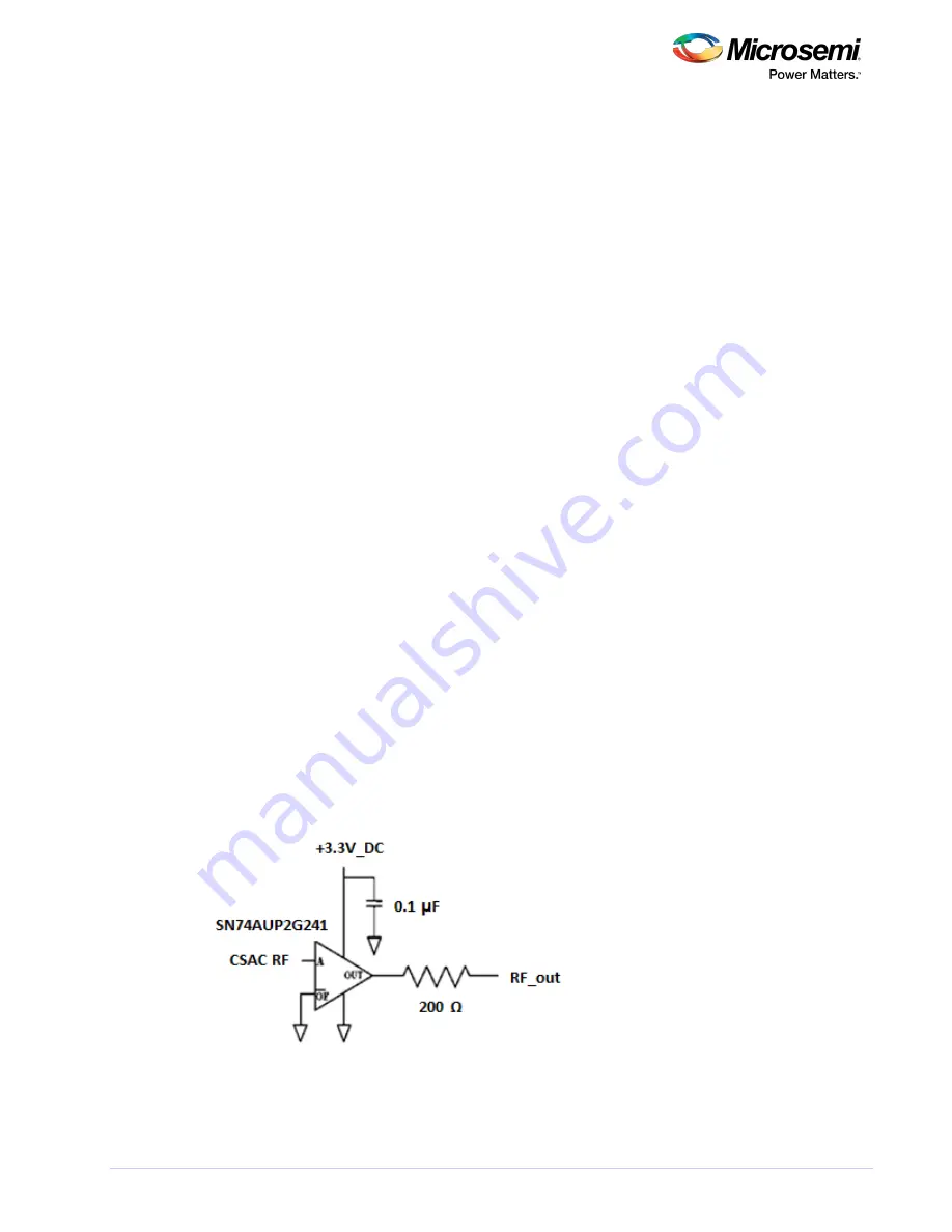
RF Output Characteristics

The buffered CMOS RF output is provided on pin 12 of the SA.45s CSAC. The output series impedance is 
200 Ω. For reference, the output driver circuit of the SA.45s is shown in the following illustration.

Figure 4 • CSAC RF Output Driver Circuit

The SA.45s is designed for embedded low-power applications—it is expected to drive a high impedance 
input, not a 50 Ω measurement instrument or transmission line.
Note: Driving a 50 Ω line at 13 dBm consumes nearly as much power as the CSAC itself. If a high-level 

Summary of Contents for SA.45s

Page 1: ...User Guide SA 45s Chip Scale Atomic Clock...

Page 2: ...Interface and Mounting Considerations 4 3 2 5 Recommended Operating Characteristics 5 3 3 Functional Description 6 3 3 1 Principle of Operation 6 3 3 2 Start Up Sequence 7 3 3 3 Built In Test Equipme...

Page 3: ...CSAC on the Test Fixture 31 3 5 4 Cabling 31 3 5 5 CSACdemo Software Installation 31 3 5 6 CSACdemo Operation 31 3 6 Data Acquisition with CSACdemo 34 3 7 Design Guide 35 3 7 1 The Art of Disciplinin...

Page 4: ...blished in August 2017 It was updated to clarify frequency steering and other edits per EC12643 1 2 Revision C Revision C was published in July 2016 It was updated to reflect 1 08 and 1 09 firmware im...

Page 5: ...ath Caution To avoid personal injury do not disregard cautions All cautions use this symbol Cautions are installation operation or maintenance procedures practices conditions or statements that if not...

Page 6: ...bility of atomic clock technology while achieving true breakthroughs in reduced size weight and power consumption The small size less than 17 cc and low power consumption of the CSAC less than 125 mW...

Page 7: ...ions All ratings apply at 25 C unless otherwise noted Table 1 Absolute Maximum Ratings Parameter Rating Supply voltage V CC 0 V 4 1 V Analog tuning voltage 0 V VCC Maximum current draw 1PPS input RS23...

Page 8: ...following table Table 3 Recommended Operating Characteristics PIN Function Level Reference Section 1 Analog tuning input1 0 V 2 5 V Analog Tuning section see page 14 4 Built in test equipment BITE 2 L...

Page 9: ...ded on the CSAC output pin 12 In normal operation the frequency of the TCXO is continuously compared and corrected to ground state hyperfine frequency of the cesium atoms contained in the physics pack...

Page 10: ...save CSAC set points to memory Otherwise upon the next power up the unit may go in to a mode of operation where it re acquires all of its set points warm up time will then be out of specification 3 3...

Page 11: ...y 1 10 Steering commands may be entered as either absolute steers or as 12 FA relative steers In the case of an absolute steer the contents of the steer register are replaced FD with the new value In...

Page 12: ...n the next polling update to indicate the internal correction of 100 10 12 The following screen shot shows an example of relative frequency tuning after absolute steer is reset to 0 In this example ea...

Page 13: ...output reflects that of the RF output Consequently when unlocked BITE 1 status 0 the 1PPS stability reflects that of the free running TCXO 3 3 8 1PPS Synchronization The 1PPS output is synchronous wit...

Page 14: ...cting a reference 1PPS signal to pin 9 without needing to issue the RS232 synchronization command Automatic synchronization can be enabled disabled through bit 3 0x0008 in the mode register see Set Cl...

Page 15: ...s frequency lock BITE 0 status 0 In the event that the 1PPS reference is removed from pin 9 while Disciplining the CSAC remains in holdover and preserves the most recent steering value If the 1PPS ref...

Page 16: ...he actual phase measurement that is if the CSAC is disciplined with 50 ns of compensation the phase meter reports 50 ns of phase error Compensation is set with the command see DC Set 1PPS Disciplining...

Page 17: ...applied at pin 1 and the resultant steering are reported in the standard telemetry stream see The tuning voltage input Telemetry 6 and see page 20 range is 0 VDC 2 5 VDC which corresponds to a full sc...

Page 18: ...ed to standard mode For example if the atomic clock portion is only powered on for 5 minutes out of every hour 2 minutes for lock acquisition 3 minutes of run time then the time averaged power of the...

Page 19: ...during sleep and unlocked cycles though steering information is preserved and updated across wake cycles Frequency Steering commands may be entered when the CSAC is asleep or unlocked but do not affec...

Page 20: ...mode may be enabled disabled through bit 2 0x0004 in the mode register see Phase Measurement mode Automatic Set Clear Operating Modes M see page 24 Synchronization and Disciplining are all mutually ex...

Page 21: ...e register see When enabled Set Clear Operating Modes M see page 24 the checksum is required for all input commands and is present on all replies from the CSAC The checksum is a two byte ASCII represe...

Page 22: ...d send in Checksum mode In MA CRLF MA 0C CRLF the following table we convert and to their binary equivalents and calculate the XOR in the bottom M A row The corresponding hexadecimal value of that XOR...

Page 23: ...r discipline status OK check m CRLF Set 1PPS Phase Threshold for Discipline Status OK Check m section see page 27 Set report 1PPS Out Pulse width as multiple of default width CRLF Set 1PPS Out Pulse W...

Page 24: ...tions 16 bits unsigned 3 digits precision 9 characters max Temp Unit temperature C Absolute accuracy is 2 C 16 bits unsigned 2 digits precision 8 characters max Steer Frequency adjust In 10 resolution...

Page 25: ...To avoid this it is recommended to always allow CSAC to remain powered on for 102 seconds after it acquires LOCK 102 seconds is the minimum amount of time necessary to save CSAC set points to memory t...

Page 26: ...d FA 123000 CRLF Unit response Steer 123 CRLF Example apply delta tuning correction of 1 23 10 10 Command FD 123000 CRLF Unit response Steer 246 CRLF Example report current value of steer Command F CR...

Page 27: ...og tuning a 0x0002 Reserved 0x0004 M 1PPS phase measurement only available on firmware versions 1 08 and later m 0x0008 S 1PPS auto sync s 0x0010 D Discipline d 0x0020 U Ultra Low Power mode u 0x0040...

Page 28: ...time constant can range between 10 to 10000 seconds The 1PPS disciplining time constant is set with the command The format for setting the time constant is D DX CRLF where X is the new time constant...

Page 29: ...minutes wake time 5 minutes Command U3300 300 CRLF Response 3300 300 CRLF The allowed ranges of Sleep Time and Wake Time are 1800 seconds to 65535 seconds and 10 seconds to 65535 seconds respectively...

Page 30: ...m The 1PPS phase threshold for discipline status OK check when disciplining to an externally supplied 1PPS reference source may be configured to provide optimal performance in a given application For...

Page 31: ...cted frequency option for RF output pin 12 When RF output frequency of 10 MHz option 001 is selected then the 1PPS out pulse width default is 100 microseconds while for other RF output frequency optio...

Page 32: ...for CRLF 3 5 Developer s Kit The CSAC Developer s Kit includes all of the necessary hardware and cabling to facilitate validation of performance brass board demonstrations and software interface deve...

Page 33: ...Developer s Kit RS232 Connection DB9M The evaluation board provides a level shifter U3 which converts the CSAC 0 VDC 3 3 VDC serial interface to the RS232 standard 12 V for direct interface with a PC...

Page 34: ...1PPS Connect either or both of these to your test equipment frequency counter spectrum analyzer and so on 3 5 5 CSACdemo Software Installation The Microsemi CSACdemo software part number 084 00365 000...

Page 35: ...tatus bar may also indicate the source of the communication failure If the COM port is in use by another application the status bar reports RS232 open failed otherwise it will likely indicate Instrume...

Page 36: ...on then off once again During acquisition the Unit Status field in the lower right corner of CSACdemo will proceed through the stages corresponding to the values of the Status register see Table 7 St...

Page 37: ...d the contrast is comfortably above 1000 3 6 Data Acquisition with CSACdemo For long term monitoring of the CSAC select the panel from the menu see Options File Figure 12 see page 19 Choose a polling...

Page 38: ...ibrate the CSAC frequency in the field even if a reference source is only occasionally or sporadically available thereby improving the long term performance phase and frequency drift of the CSAC At th...

Page 39: ...minates for 5000 seconds and the superior GPS stability dominates for 5000 seconds On the other hand consider the case where the CSAC is disciplined to a high performance cesium clock which is more st...

Page 40: ...nd therefore produces little heat Furthermore the external parts of CSAC are mu metal 80 nickel which is a poor thermal conductor 1 5 that of aluminum There is no useful thermal path from the inside c...

Page 41: ...e signal as needed by the user VCC for the UHS inverter is supplied with a resistor divider and Darlington pair to provide a good filter for removing 50 Hz 60 Hz AC line noise However caution must be...

Page 42: ...anges mode register format where x is an Mx alphabetical character in list below causes an NVRAM write RS232 Communications Checksum on off vs MC Mc External oscillator on off vs MZ Mz PPS auto sync o...

Page 43: ...y to independently determine suitability of any products and to test and verify the same The information provided by Microsemi hereunder is provided as is where is and with all faults and the entire r...

Page 44: ...Mouser Electronics Authorized Distributor Click to View Pricing Inventory Delivery Lifecycle Information Microchip 990 00123 000...

Reviews: