SyncLink PCIe Serial Adapter
Hardware
User’s Manual
MicroGate Systems, Ltd
http://www.microgate.com
MicroGate® and SyncLink® are registered trademarks of MicroGate Systems, Ltd.
Copyright © 2008-2020 MicroGate Systems, Ltd. All Rights Reserved
Page 1: ...rial Adapter Hardware User s Manual MicroGate Systems Ltd http www microgate com MicroGate and SyncLink are registered trademarks of MicroGate Systems Ltd Copyright 2008 2020 MicroGate Systems Ltd All...
Page 2: ...ations 5 Single Ended Signals RS 232 V 28 5 Differential Signals RS 422 RS 485 V 11 5 Clock Polarity 6 Serial Interface and Termination Selection 7 Serial Connector Pin Assignments 8 RS 232 8 V 35 9 R...
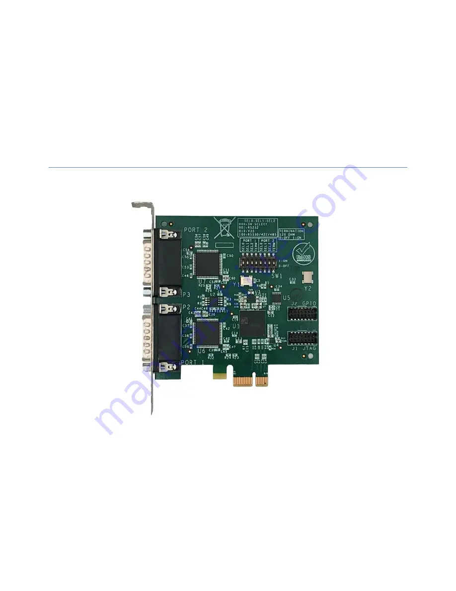
Page 3: ...2 485 RS 530 RS 449 X 21 Optional termination for differential inputs Full set of control and status signals DTR DSR RTS CTS DCD RI LL RL Specifications MicroGate FPGA serial controller 2 ports PCI Ex...
Page 4: ...port Adapter cables are included with the card to convert each 26 pin connector into a standard DB 25 male connector Port 1 is closest to the PCIe edge connector Port numbers are labeled on the board...
Page 5: ...ential signals are compatible with RS 422 RS 485 and ITU V 11 standards Each signal has two connector pins named A and B These pins are also named but this convention can be inverted depending on cont...
Page 6: ...On to Off edge falling edge receive data sample bit center Off to On edge rising edge transmit data transition bit edge RS 422 RS 485 V 11 Differential Signals 200mV to 6V 2V typical clock on 200mV t...
Page 7: ...preventing software modification The TERM switch controls the 120 ohm termination option for differential inputs RS 530 422 485 V 11 on a port Single ended inputs RS 232 V 28 never use termination reg...
Page 8: ...signals on a DB 25 connector Use a straight through 25 conductor DB 25M to DB 25F cable such as MicroGate Part CMF000 Maximum data rate is 128Kbps Cable length and signal loading may reduce the maxim...
Page 9: ...ut RTS Request to Send RS 232 V 28 1 4 C Output CTS Clear to Send RS 232 V 28 24 5 D Input DSR Data Set Ready RS 232 V 28 19 6 E Input Signal Ground 14 7 B DCD Data Carrier Detect RS 232 V 28 22 8 F I...
Page 10: ...to Send RS 422 V 11 24 5 9 Input DSR A Data Set Ready RS 422 V 11 19 6 11 Input Signal Ground 14 7 19 DCD A Data Carrier Detect RS 422 V 11 22 8 13 Input RxC B Receive Clock RS 422 V 11 11 9 26 Input...
Page 11: ...V 11 8 2 2 Output R A Receive Data RS 422 V 11 17 3 4 Input I A Indicator DSR DCD RS 422 V 11 19 22 6 8 5 Input Signal Ground 14 7 8 S B Clock Input TxC RxC RS 422 V 11 11 26 9 12 13 Input I B Indica...
Page 12: ...TL compatible and inputs are 5V tolerant Exceeding specifications can damage the card GPIO Pin Assignments Pin Description 1 Ground 2 GCK0 Dedicated special purpose LVTTL input Leave unconnected 3 GPI...
Page 13: ...is made by Integrated Device Technologies IDT Refer to the documentation available from IDT www idt com for details on programming the synthesizer An IDT supplied program Versaclock generates program...