background image

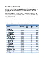
GPIO


Pin


Assignments


Pin


#


Description


1


Ground


2


GCK0


Dedicated


special


purpose


LVTTL


input


Leave


unconnected


3


GPIO[6]


4


GPIO[0]


5


GPIO[7]


6


GPIO[1]


7


GPIO[8]


8


GPIO[2]


9


GPIO[9]


10


GPIO[3]


11


GPIO[10]


12


GPIO[4]


13


GPIO[11]


14


GPIO[5]


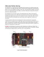
The


GT


adapter


has


a


total


of


12


general


purpose


I/O


signals


(GPIO[0]


to


GPIO[11]).


By


default


on


power


up


all


GPIO


signals


are


configured


as


inputs


(direction


control


=


0).


Refer


to


the


serial


API


documentation


for


details


on


configuring


and


using


GPIO


signals.


WARNING:


Take


care


when


connecting


to


GPIO


signals


to


prevent


damage


to


the


serial


card.


Outputs


should


only


be


connected


to


inputs


and


not


other


outputs.


Voltage


limits


as


shown


above


should


not


be


exceeded.


Summary of Contents for SyncLink GT2

Page 1: ...Serial Adapter Hardware User s Manual MicroGate Systems Ltd http www microgate com MicroGate and SyncLink are registered trademarks of MicroGate Systems Ltd Copyright 2008 2012 MicroGate Systems Ltd All Rights Reserved ...

Page 2: ... V 28 5 Differential Signals RS 422 RS 485 V 11 5 Clock Polarity 5 Serial Interface Selection 7 Differential Input Termination 8 Differential Fail Safe Biasing 9 Serial Connector Pin Assignments 10 RS 232 11 V 35 12 RS 422 RS 449 RS 485 RS 530 13 X 21 15 General Purpose I O Signals 16 DC GPIO Specifications 16 ...

Page 3: ... NRZI NRZ M NRZ S FM0 FM1 Manchester differential biphase level Selectable interface for RS 232 V 35 RS 422 485 RS 530 RS 449 X 21 Optional termination for differential inputs Optional fail safe biasing for differential inputs Full set of control and status signals DTR DSR RTS CTS DCD RI LL RL Specifications MicroGate FPGA serial controller 2 or 4 ports PCI 3 0 compatible with 5V 3 3V and PCI X sl...

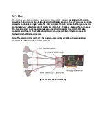
Page 4: ...to convert each 60 pin connector into two standard DB 25 male connectors The GT2 card uses one 60 pin connector and includes a single Y cable for a total of 2 ports The GT4 card uses both 60 pin connectors and includes two Y cables for a total of 4 ports Each branch of a Y cable is labeled with a port number The Y cable labeled 1 and 2 should be installed on the 60 pin connector closest to the PCI...

Page 5: ...ate Differential Signals RS 422 RS 485 V 11 Differential signals supported by the card are compatible with RS 422 RS 485 and ITU V 11 standards Each differential signal uses two conductors in a cable signal pair A common ground conductor is recommended for use with differential signals to reduce common mode voltages between cable ends which may result in incorrect or impaired operation Maximum Vol...

Page 6: ...nsmit data transition bit edge RS 422 RS 485 V 11 Differential Signals 200mV to 5V 2V typical clock on 200mV to 5V 2V typical clock off On to Off edge falling edge receive data sample bit center Off to On edge rising edge transmit data transition bit edge Most serial communications equipment uses the above clock polarity but some non standard equipment may use the opposite polarity For differentia...

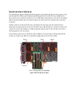
Page 7: ...he connected communications equipment Interface selection is preset at the factory as specified by the ordering code The selection may be changed by moving the jumpers to the desired header row as described above Use pliers to remove the jumpers from the current position carefully working the jumpers loose from the headers Take care to not damage the card or cause injury Some interface types requi...

Page 8: ...eds receivers at each end of a cable should be terminated For a multi drop setups more than 2 devices on a cable do not terminate receivers connected to the middle of the cable At slower speeds the termination can usually remain without problem Removing termination at slower speeds may allow the use of longer cables To remove a termination resistor pack identify the socket labeled TERM Then remove...

Page 9: ...uit maintains the input in a steady state When an input is terminated external fail safe biasing resistor pack may be required to guarantee the input is in a steady state An example application that uses fail safe biasing is bus mode connections where a single cable conductor pair is connected to both the transmit data output and receive data input for more than one station In this setup only one ...

Page 10: ...nectors The assignment of signals to the connector pins is controlled by the interface selection jumpers on the card For interface types that use a connector different than DB 25 an adapter cable purchased from MicroGate is required The following sections describe the jumper settings and cables for each supported standard ...

Page 11: ...value RS 232 DB 25 Male DTE Signal Name Electrical Desc Pin Direction Earth Shield Ground 1 TxD Transmit Data RS 232 V 28 2 Output RxD Receive Data RS 232 V 28 3 Input RTS Request to Send RS 232 V 28 4 Output CTS Clear to Send RS 232 V 28 5 Input DSR Data Set Ready RS 232 V 28 6 Input Signal Ground 7 DCD Data Carrier Detect RS 232 V 28 8 Input TxC Transmit Clock RS 232 V 28 15 Input RxC Receive Cl...

Page 12: ...th Shield Ground 1 A TxD A Transmit Data RS 422 V 11 2 P Output RxD A Receive Data RS 422 V 11 3 R Input RTS Request to Send RS 232 V 28 4 C Output CTS Clear to Send RS 232 V 28 5 D Input DSR Data Set Ready RS 232 V 28 6 E Input Signal Ground 7 B DCD Data Carrier Detect RS 232 V 28 8 F Input RxC B Receive Clock RS 422 V 11 9 X Input AuxClk B DTE Clock Output RS 422 V 11 11 W Output TxC B Transmit ...

Page 13: ...is value RS 422 RS 530 RS 449 Male DTE Signal Name Electrical Desc DB25 RS 530 Pin DB37 RS 449 Pin Direction Earth Shield Ground 1 1 TxD A Transmit Data RS 422 V 11 2 4 Output RxD A Receive Data RS 422 V 11 3 6 Input RTS A Request to Send RS 422 V 11 4 7 Output CTS A Clear to Send RS 422 V 11 5 9 Input DSR A Data Set Ready RS 422 V 11 6 11 Input Signal Ground 7 19 DCD A Data Carrier Detect RS 422 ...

Page 14: ...Figure 7 RS 530 Cable Part CMF000 Figure 8 RS 449 Cable Part 2537FM ...

Page 15: ...ximum usable data rate from this value X 21 Male DTE Signal Name Electrical Desc DB25 Pin DB15 Pin Direction Earth Shield Ground 1 1 T Transmit Data RS 422 V 11 2 2 Output R Receive Data RS 422 V 11 3 4 Input I Indicator DSR DCD RS 422 V 11 6 8 5 Input Signal Ground 7 8 S Clock Input TxC RxC RS 422 V 11 9 12 13 Input I Indicator DSR DCD RS 422 V 11 10 22 12 Input X Clock Output AuxClk RS 422 V 11 ...

Page 16: ...erial API Windows and Linux Each signal can be configured to be either an input or an output Inputs can be monitored and outputs can be controlled DC GPIO Specifications Vil input low 0 5V min 0 8V max Vih input high 2 0V min 5 5V max Vol output low 0 4V max Voh output high 2 4V min Iol output low 24mA max Iil output high 24mA max Input Current 10uA max GPIO signals are 3 3V TTL compatible and inp...

Page 17: ...has a total of 12 general purpose I O signals GPIO 0 to GPIO 11 By default on power up all GPIO signals are configured as inputs direction control 0 Refer to the serial API documentation for details on configuring and using GPIO signals WARNING Take care when connecting to GPIO signals to prevent damage to the serial card Outputs should only be connected to inputs and not other outputs Voltage lim...

Page 18: ......

Reviews: