27
Chapter 6
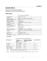
Specifications
Typical for 25 °C unless otherwise specified.
Specifications in
italic text
are guaranteed by design.
Analog input
Table 1. Analog input specifications
A/D converter type
Successive approximation
Resolution 16-bits
Number of channels
16 single-ended/8 differential, software selectable
Input ranges (SW programmable)
Bipolar: ±10 V, ±5 V, ±2 V, ±1 V , ±0.5 V, ±0.2 V, ±0.1 V
Maximum sample rate
1 MHz
Nonlinearity (integral)
±2 LSB maximum
Nonlinearity (differential)
±1 LSB maximum
A/D pacing
Onboard A/D clock, external source (XAPCR)
Trigger sources and modes
Data transfer
DMA
Configuration memory
Programmable I/O
Maximum usable input voltage
+ common mode voltage
(CMV + V
in
)
Range: ±10 V, ±5 V, ±2 V, ±1 V , ±0.5 V
10.5 V maximum
Range: ±0.2 V, ±0.1 V
2.1 V maximum
Signal to noise and distortion
72 dB typical for ±10 V range, 1 kHz fundamental
Total harmonic distortion
-80 dB typical for ±10 V range, 1 kHz fundamental
Calibration
Auto-calibration, calibration factors for each range stored onboard in non-volatile
RAM.
CMRR @ 60 Hz
-70 dB typical DC to 1 kHz
Bias current
40 pA typical (0°C to 35°C)
Input impedance
10 M
Ω
single-ended, 20 M
Ω
differential
Absolute maximum input voltage
±30 V
Accuracy
Table 2. Analog input accuracy specifications
Voltage range
Accuracy
±(% of r %
range)
23°C ±10 °C, 1 year
Temperature coefficient
±(ppm of r ppm
range)/°C
Noise (cts RMS)
-10 V to 10 V
0.031% + 0.008%
14 + 8
1.5
-5 V to 5 V
0.031% + 0.009%
14 + 9
2.0
-2 V to 2 V
0.031% + 0.010%
14 +10
1.6
-1 V to 1 V
0.031% + 0.02%
14 + 12
2.5
-500 mV to 500 mV
0.031% + 0.04%
14 +18
4.0
-200 mV to 200 mV
0.036% + 0.075%
14 +12
5.0
-100 mV to 100 mV
Note 1
0.042% + 0.15%
14 +18
9.0
Note 2
Note 1:
Specifications assume differential input single-channel scan, 1 MHz scan rate, unfiltered,
CMV=0.0 V, 30 minute warm-up, exclusive of noise.
Note 2:
Noise reflects 10,000 samples at 1 MHz, typical, differential short, using CA-68-3S cable.
Summary of Contents for PCI-2515
Page 1: ......

