Maxim DS80C400 User Manual Download Page 95

DS80C400 Network Microcontroller 


95 of 96 

source to exit stop mode, resuming operation in less than 100ns. After 65,536 oscillations of the external clock 
source (not the ring oscillator), the device clears the ring oscillator mode bit, RGMD (EXIF.2), to indicate that the 
device has switched from the ring oscillator to the external clock source. 

The ring oscillator runs at approximately 15MHz, but varies over temperature and voltage. As a result, no serial 
communication or precision timing should be attempted while running from the ring oscillator, since the operating 
frequency is not precise. Likewise, the Ethernet and CAN controllers derive their timing from the system clock and 
should not be enabled until RGMD = 0. The reset (default) state of the RGSL bit is logic 0, which does not result in 
use of the ring oscillator to exit stop mode. 
 

EMI Reduction  

One of the major contributors to radiated noise in an 8051-based system is the toggling of ALE. The microcontroller 
allows software to disable ALE when not used by setting the ALEOFF (PMR.2) bit to a 1. When ALEOFF = 1, ALE 
automatically toggles during off-chip program and data memory accesses. However, ALE remains static when 
performing on-chip memory access. The default state of ALEOFF is 0, so ALE normally toggles at a frequency of 
XTAL/4. 
 

Software Breakpoint Mode 

The DS80C400 provides a special software-breakpoint mode for code-debug purposes. Breakpoint mode can be 
enabled by setting the BPME bit (ACON.4) to a logic 1. Once enabled, the A5h op code can be used to create a 
break in code execution. When the break op code (A5h) is executed, all clocks to the timer 0, 1, 2, 3, and watchdog 
timer blocks are stopped and any serial port operation (when derived from a timer) is halted. Additionally, the state 
machine controlling access to timed-access-protected SFRs is suspended. Much like an interrupt, the CPU 
generates a hardware LCALL and vector to address location 000083h. Unlike an interrupt, however, the return 
address is not pushed onto the stack, but is placed into the BPA1 (LSB), BPA2 (MSB), and BPA3 (XSB) SFRs, and 
the A5h op code is used to exit breakpoint mode and return to the address contained in the BPA3:1 SFRs.  
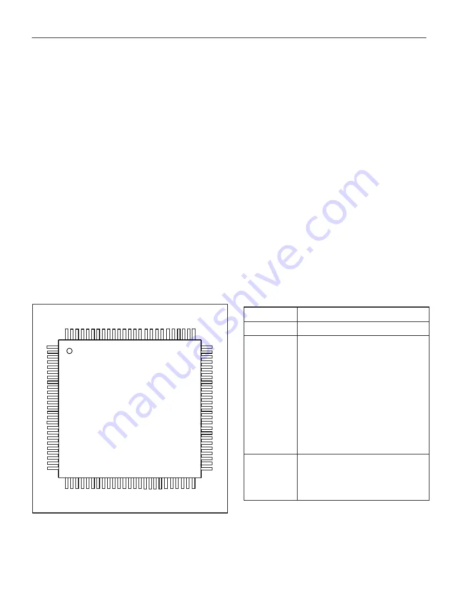
 

PIN CONFIGURATION 


REVISION HISTORY 

REVISION DESCRIPTION 

111202 

New product release 

060203 

Replaced “DS2502U-E48” with 
“DS2502-E48.” 

MOVX Characteristics (Nonmultiplexed 
Address/Data Bus) 

table: Moved MIN 

spec for t

PXIZ

 to MAX column. 

Added note for connecting the PHY to 
the DS80C400: “When connecting the 
DS80C400 to an external PHY, do not 
connect the 

RSTOL

 to the reset of the 

PHY. Doing so may disable the 
Ethernet transmit.” 

Updated 

Figure 12: ROM Code Boot 

Sequence

 flowchart. 

102103 

Corrected 

PSEN

 signal in the 

“Nonmultiplexed, 2-Cycle Data Memory 

CE0-7

 Write” timing diagram. 

Corrected PT2/PT3 references in Table 
21 and Table 28. 


100 

76

50

26 

Dallas 

Semiconductor 

DS80C400 

75

51

25 

TOP VIEW 

LQFP 

Summary of Contents for DS80C400

Page 1: ...Terminals ORDERING INFORMATION PART TEMP RANGE MAX CLOCK SPEED PIN PACKAGE DS80C400 FNY 40 C to 85 C 75MHz 100 LQFP 1 Wire is a registered trademark of Dallas Semiconductor Magic Packet is a trademar...

Page 2: ...for XTAL1 RST OW VIL2 1 0 V Input High Level VIH1 2 0 V Input High Level for XTAL1 RST OW VIH2 2 4 V Output Low Current for Port 1 3 7 at VOL 0 4V IOL1 6 10 mA Output Low Current for Port 0 2 TX_EN T...

Page 3: ...um at approximately 2V Note 12 During external addressing mode weak latches are used to maintain the previously driven state on the pin until such time that the Port 0 pin is driven by an external mem...

Page 4: ...or is used in conjunction with the default system clock selection CD1 CD0 10b the minimum maximum system clock high tCHCL and system clock low tCLCH periods are directly related to clock oscillator du...

Page 5: ...RD or PSEN or WR High to ALE tWHLH 5tCLCL 3 5tCLCL 4 ns 4 CST 7 tCHCL 5 tCHCL 13 CST 0 tCLCL tCHCL 5 tCLCL tCHCL 13 1 CST 3 RD or PSEN or WR High to Port 4 CE or Port 5 PCE High tWHLH2 5tCLCL tCHCL 5...

Page 6: ...DS80C400 Network Microcontroller 6 of 96...

Page 7: ...DS80C400 Network Microcontroller 7 of 96...

Page 8: ...6 MULTIPLEXED 2 CYCLE DATA MEMORY PCE0 3 READ MULTIPLEXED 2 CYCLE DATA MEMORY CE0 7 READ PORT 4 3 CE0 PORT 4 6 ADDRESS PORT 6 7 CE4 A16 A21 A16 A21 A16 A21 A16 A21 PORT 4 3 CE0 PORT 6 7 CE4 PORT 4 6 A...

Page 9: ...TIPLEXED 2 CYCLE DATA MEMORY CE0 7 WRITE MULTIPLEXED 3 CYCLE DATA MEMORY PCE0 3 READ OR WRITE PORT 4 3 CE0 PORT 6 7 CE4 PORT 4 6 ADDRESS A16 A21 A16 A21 A16 A21 A16 A21 PORT 4 3 CE0 PORT 6 7 CE4 PORT...

Page 10: ...96 MULTIPLEXED 3 CYCLE DATA MEMORY CE0 7 READ MULTIPLEXED 3 CYCLE DATA MEMORY CE0 7 WRITE PORT 4 3 CE0 PORT 6 7 CE4 PORT 4 6 ADDRESS A16 A21 A16 A21 A16 A21 A16 A21 PORT 4 3 CE0 PORT 6 7 CE4 PORT 4 6...

Page 11: ...LTIPLEXED 9 CYCLE DATA MEMORY PCE0 3 READ OR WRITE MULTIPLEXED 9 CYCLE DATA MEMORY CE0 7 READ PORT 4 3 CE0 PORT 6 7 CE4 PORT 4 6 ADDRESS A16 A21 A16 A21 A16 A21 A16 A21 PORT 4 3 CE0 PORT 6 7 CE4 PORT...

Page 12: ...DS80C400 Network Microcontroller 12 of 96 MULTIPLEXED 9 CYCLE DATA MEMORY CE0 7 WRITE PORT 4 3 CE0 PORT 6 7 CE4 PORT 4 6 ADDRESS A16 A21 A16 A21 A16 A21 A16 A21...

Page 13: ...LCH 19 ns Note 1 Specifications to 40 C are guaranteed by design and not production tested Note 2 All parameters apply to both commercial and industrial temperature operation unless otherwise noted No...

Page 14: ...or PSEN or WR Low tAVWL1 10tCLCL 5 ns 4 CST 7 tCLCL tCLCH 5 CST 0 2tCLCL tCLCH 5 1 CST 3 Port 2 4 6 Address Port 4 CE or Port 5 PCE to RD or PSEN or WR Low tAVWL2 10tCLCL tCLCH 5 ns 4 CST 7 Data Vali...

Page 15: ...DS80C400 Network Microcontroller 15 of 96...

Page 16: ...DS80C400 Network Microcontroller 16 of 96 l...

Page 17: ...PLEXED 2 CYCLE DATA MEMORY PCE0 3 READ OR WRITE NONMULTIPLEXED 2 CYCLE DATA MEMORY CE0 7 READ PORT 4 3 CE0 PORT 6 7 CE4 PORT 4 6 ADDRESS A16 A21 A16 A21 A16 A21 A16 A21 PORT 4 3 CE0 PORT 6 7 CE4 PORT...

Page 18: ...ED 2 CYCLE DATA MEMORY CE0 7 WRITE NONMULTIPLEXED 3 CYCLE DATA MEMORY PCE0 3 READ OR WRITE PORT 4 3 CE0 PORT 6 7 CE4 PORT 4 6 ADDRESS A16 A21 A16 A21 A16 A21 A16 A21 PORT 7 PORT 4 3 CE0 PORT 6 7 CE4 P...

Page 19: ...IPLEXED 3 CYCLE DATA MEMORY CE0 7 READ NONMULTIPLEXED 3 CYCLE DATA MEMORY CE0 7 WRITE PORT 4 3 CE0 PORT 6 7 CE4 PORT 4 6 ADDRESS A16 A21 A16 A21 A16 A21 A16 A21 PORT 7 PORT 4 3 CE0 PORT 6 7 CE4 PORT 4...

Page 20: ...ED 9 CYCLE DATA MEMORY PCE0 3 READ OR WRITE NONMULTIPLEXED 9 CYCLE DATA MEMORY CE0 7 READ PORT 4 3 CE0 PORT 6 7 CE4 PORT 4 6 ADDRESS A16 A21 A16 A21 A16 A21 A16 A21 PORT 7 PORT 4 3 CE0 PORT 6 7 CE4 PO...

Page 21: ...t tSLOT 68 8 86 12 15 68 8 86 ms Low Time for Write 1 tLOW1 4 8 6 0 8 1 7 2 9 ms Low Time for Write 0 tLOW0 62 4 78 8 10 62 4 78 ms Write Data Sampling Time tWDV 15 60 2 6 25 60 ms Read Data Sampling...

Page 22: ...DS80C400 Network Microcontroller 22 of 96 OW PIN TIMING...

Page 23: ...nd receiving bits within a byte The difference comes when the last bit of the byte has been completely sent At this point the signal is either enabled continuously until the next reset or time slot be...

Page 24: ...D TX_EN Data Setup to TXClk tTSU 10 25 ns TXD TX_EN Data Hold from TXClk tTHD 2 2 ns RXClk Pulse Width tRDC 14 26 140 260 ns RXClk to RXD RX_DV RX_ER Valid tRDV 10 30 190 210 ns MDC Period tMCLCL 400...

Page 25: ...ycle 10 tCLCL 10 Output Data Setup to Clock Rising tQVXH SM2 1 4 clocks per cycle 3 tCLCL 10 ns SM2 0 12 clocks per cycle 2 tCLCL 10 Output Data Hold from Clock Rising tXHQX SM2 1 4 clocks per cycle t...

Page 26: ...DS80C400 Network Microcontroller 26 of 96 SERIAL PORT 0 SYNCHRONOUS MODE TRADITIONAL 8051 OPERATION TXD CLOCK XTAL 12 SM2 0 HIGH SPEED OPERATION TXD CLK SYSCLK 4 SM2 1...

Page 27: ...536 tCLCK Note 1 Startup time for crystals varies with load capacitance and manufacturer Time shown is for an 11 0592MHz crystal manufactured by Fox Electronics Note 2 Reset delay is a synchronous cou...

Page 28: ...0 CONTROLLER CAN SRAM 256 x 8 BUFFER CONTROL UNIT ACCUMULATOR PORT LATCH PORT 4 OSCILLATOR PORT 2 PORT LATCH PORT 0 1 WIRE CONTROLLER PORT LATCH SRAM 9kk x 8 V CC POWER MONITOR RESET CONTROL OSCILLAT...

Page 29: ...rystal amplifier 86 AD0 D0 85 AD1 D1 84 AD2 D2 83 AD3 D3 82 AD4 D4 81 AD5 D5 80 AD6 D6 79 AD7 D7 AD0 7 Port 0 I O When the MUX pin is connected low Port 0 is the multiplexed address data bus While ALE...

Page 30: ...n driver followed by a weaker sustaining pullup Once the momentary strong driver turns off the port once again becomes the output and input high state Port Alternate Function P4 0 CE0 Program Memory C...

Page 31: ...ion of frames 10 RXClk Receive Clock Input The receive clock is a continuous clock sourced from the Ethernet PHY controller It is used to provide timing reference for transferring of RX_DV RX_ER and R...

Page 32: ...6 network stack and OS are provided in ROM The network stack supports up to 32 simultaneous TCP connections and can transfer up to 5Mbps through the Ethernet MAC Its maximum system clock frequency of...

Page 33: ...the ability to place the CPU into an idle state or an ultra low power stop mode state As protection against brownout and power fail conditions the microcontroller is capable of issuing an early warni...

Page 34: ...0 a machine cycle requires only 4 clocks Thus the fastest instruction 1 machine cycle in duration executes three times faster for the same crystal frequency The majority of instructions on the DS80C40...

Page 35: ...7 A15 P2 6 A14 P2 5 A13 P2 4 A12 P2 3 A11 P2 2 A10 P2 1 A9 P2 0 A8 A0h P5 P5 7 PCE3 P5 6 PCE2 P5 5 PCE1 P5 4 PCE0 P5 3 P5 2 T3 P5 1 C0RX P5 0 C0TX A1h P5CNT CAN0BA C0_I O P5CNT 2 P5CNT 1 P5CNT 0 A2h...

Page 36: ...4X 2X ALEOFF C4h STATUS PIP HIP LIP SPTA1 SPRA1 SPTA0 SPRA0 C5h MCON IDM1 IDM0 CMA PDCE3 PDCE2 PDCE1 PDCE0 C6h TA C7h T2CON TF2 EXF2 RCLK TCLK EXEN2 TR2 C T2 CP RL2 C8h T2MOD D13T1 D13T2 T2OE DCEN C9h...

Page 37: ...ID3 ID2 F6h STATUS1 V1PF V3PF SPTA2 SPRA2 F7h EIP EPMIP C0IP EAIP PWDI PWPI PS2 PT3 PX2 5 F8h P7 P7 7 A7 P7 6 A6 P7 5 A5 P7 4 A4 P7 3 A3 P7 2 A2 P7 1 A1 P7 0 A0 F9h TL3 FBh TH3 FCh T3CM TF3 TR3 T3M S...

Page 38: ...0 0 0 9Ch ACON 1 1 0 0 Special 0 0 0 9Dh C0TMA0 0 0 0 0 0 0 0 0 9Eh C0TMA1 0 0 0 0 0 0 0 0 9Fh P2 1 1 1 1 1 1 1 1 A0h P5 1 1 1 1 1 1 1 1 A1h P5CNT 1 0 0 0 0 0 0 0 A2h C0C 0 0 0 0 1 0 0 1 A3h C0S 0 0 0...

Page 39: ...0 0 DBh BPA3 0 0 0 0 0 0 0 0 DCh ACC 0 0 0 0 0 0 0 0 E0h OCAD 0 0 0 0 0 0 0 0 E1h CSRD 0 0 0 0 0 0 0 0 E3h CSRA 0 0 0 0 0 0 0 0 E4h EBS 0 1 1 0 0 0 0 0 E5h BCUD 0 0 0 0 0 0 0 0 E6h BCUC 0 0 0 0 0 0 0...

Page 40: ...ation Bits MCON 5 CAN CMA Data Memory Assignment MCON 3 0 PDCE3 PDCE0 Program Data Chip Enables COR CEh COR 7 IRDACK IRDA Clock Output Enable COR 4 3 C0BPR7 C0BPR6 CAN 0 Baud Rate Prescale Bits COR 2...

Page 41: ...hing instructions automatically save and restore the entire program counter The 24 bit branching instructions such as ACALL AJMP LCALL LJMP MOV DPTR RET and RETI instructions require an assembler comp...

Page 42: ...A2h and Port 6 control register P6CNT B2h designate the number of peripheral chip enables and the maximum amount of addressable data memory per peripheral chip enable Table 5 shows which port pins ar...

Page 43: ...y space are disabled Write access to combined program and data memory blocks is controlled by the WR signal and read access is controlled by the PSEN signal This feature is especially useful if the de...

Page 44: ...n data pointer related instructions toggle the active data pointer selection to the other pointer in the pair Enabling the auto toggle feature with one pointer to source data and a second pointer to d...

Page 45: ...he active data pointer after certain DPTR based instructions are executed This feature can greatly reduce the software overhead associated with data memory block moves which toggle between the source...

Page 46: ...ng accessed The default of one stretch cycle allows the use of commonly available SRAMs without dramatically lengthening the memory access times Stretch cycle settings affect external MOVX timing in t...

Page 47: ...ory accesses do not generate WR or RD strobes The DS80C400 contains an additional 256 Bytes of internal SRAM that is used to configure and operate the 15 CAN controller message centers The address loc...

Page 48: ...MULTIPLY 16 x 16 Load MA with dividend LSB Load MA with dividend LSB 1 Load MA with dividend LSB 2 Load MA with dividend MSB Load MB with divisor LSB Load MB with divisor MSB Poll the MST bit until cl...

Page 49: ...le before attempting a transmission Having multiple stations on the network results in the possibility of transmissions from different stations colliding When a collision is detected the MAC waits som...

Page 50: ...TER ADDRESS CSRA FUNCTION 00h MAC Control 04h Ethernet MAC Physical Address 47 32 08h Ethernet MAC Physical Address 31 0 0Ch Multicast Address Hash Table 63 32 10h Multicast Address Hash Table 31 0 14...

Page 51: ...ndled by the application code Command Status CSR Registers The CSR registers are essential in defining the operational characteristics of the Ethernet controller The CSR registers contain the followin...

Page 52: ...mode and has no affect on MII mode operation 0 heart beat signal quality generator function enabled default 1 heart beat signal quality generator function is disabled PS Port Select 0 MII mode defaul...

Page 53: ...t filter bit in the receive status word is set 1 for each broadcast frame received default 1 packet filter bit in the receive status word is reset 0 for each broadcast frame received DRTY Disable Retr...

Page 54: ...m MAC Physical Address 47 32 These two bytes represent the 16 most significant bits of the MAC physical address CSR Register MAC Address Low Register Address 08h Bit Names 31 PADR 31 24 24 23 PADR 23...

Page 55: ...64 bit hash table that are used for hash table filtering The multicast hash filtering mode is detailed later in the data sheet CSR Register Multicast Address Low Register Address 10h Bit Names 31 HT...

Page 56: ...eration is to be requested of the addressed PHY PHY register 0 read 1 write BUSY Busy This status bit indicates when PHY communication is currently taking place on the MII serial management bus The ap...

Page 57: ...MAC decodes if FCE 1 but does not set the receive status word packet filter bit default 1 MAC decodes if FCE 1 and sets the packet filter bit 1 for pause control frames FCE Flow Control Enable 0 MAC...

Page 58: ...ne whether it is a VLAN1 frame If a non zero match occurs the max frame length is extended from 1518 Bytes to 1522 Bytes CSR Register VLAN2 Tag Register Address 24h Bit Names 31 24 23 16 15 VLAN2 15 8...

Page 59: ...U Global Unicast 0 frames must pass the destination address filter as well as the wake up frame filter criteria in order to generate a wake up event default 1 frames must pass only the wake up frame f...

Page 60: ...g edge of clock MDC The MII address 14h and MII data 18h CSR registers outlined previously in the CSR Register section are used by the CPU to monitor and control the 2 wire MII serial bus A write to t...

Page 61: ...ect input is required for half duplex operation to signal when a collision has occurred on the physical media Ethernet Frames The basic purpose of the MII I O block is to deliver and receive Ethernet...

Page 62: ...ter possibilities exist perfect inverse and hash Perfect filtering requires that the destination address perfectly match the MAC physical address that has been assigned in CSR registers MAC address hi...

Page 63: ...ming TPID occupy the 13th and 14th byte positions those that would normally contain either the length or type field for the frame The TPID is compared against the VLAN1 20h and VLAN2 24h CSR registers...

Page 64: ...receive data packets can span multiple pages The reset default state of the Ethernet buffer size select bits EBS 4 EBS 0 is 00000b which configures all 32 pages as transmit buffer memory As an exampl...

Page 65: ...llision Observed This bit is only valid in half duplex mode and is always set if the late collision abort LTCOL bit is set in the status word 0 no late collisions observed 1 late collision collision a...

Page 66: ...il 0 destination address of the current receive frame passed the applied address filter 1 destination address of the current receive frame failed the applied address filter BCF Broadcast Frame 0 recei...

Page 67: ...valid for runt frames less than 14 Bytes 0 length specified in the length type field i e value equal or less than 1500 1 type specified in the length type field i e value greater than 1500 COL Collisi...

Page 68: ...PMF of the BCUC SFR should be cleared and if the Enable Sleep Mode command was used to invoke sleep mode then the Disable Sleep Mode command must be issued Magic Packet and Network Wake Up Frame The p...

Page 69: ...ontrols are the EA pin and the bypass ROM BROM SFR bit No matter the state of the BROM bit if the EA pin is held at a logic low level the TINI400 ROM code is not entered and is not accessible to the u...

Page 70: ...e 12 ROM Code Boot Sequence N Y EA PIN ROM INIT RESET STATE NETBOOT BROM BIT POWER ON RESET BROM 0 SERIAL LOADER P1 7 PIN NETBOOT P5 3 PIN AUTO BAUD SUCCESS SERIAL LOADER FIND USER CODE RUN USER CODE...

Page 71: ...ables PCE0 3 P5CNT 07h Enables CE4 7 1M peripheral chip enable P6CNT 27h Merged program data CE0 3 relocate internal XRAM MCON AFh Enables extended 1kB stack option ACON 2 1 Configure to maximum MOVX...

Page 72: ...A summary of the supported serial loader commands can be seen in Table 17 A detailed description of each command and further information pertaining to the serial loader can be found in the High Speed...

Page 73: ...should then respond with an IP address offering The DS80C400 subsequently requests the IP address to which the DHCP server must acknowledge In the DHCP acknowledge packet the TFTP server IP address is...

Page 74: ...CRC 16 differs it performs a couple of write read back operations to assess whether the bank is flash or SRAM and then executes the erasure if flash and programming After completion of the TFTP server...

Page 75: ...is fixed at addresses FF0002h XSB FF0003h MSB and FF0004h LSB The first three bytes of the export table contain the quantity of function entries in the export table In 3 Byte increments following the...

Page 76: ...nnect 22 bind 23 listen 24 accept 25 recv 26 send 27 getsockopt 28 setsockopt 29 getsockname 30 getpeername 31 cleanup 32 avail 33 join 34 leave 35 ping 36 getnetworkparams 37 setnetworkparams 38 geti...

Page 77: ...t 79 WOS_Tick Timer interrupt handler 80 BLOB Start address of the memory area ignored by NetBoot 81 WOS_IOPoll Asynchronous TCP IP maintenance functions 82 IP_ProcessReceiveQueues 83 IP_ProcessOutput...

Page 78: ...t to the specified address port listen Listens for connections on the specified socket accept Accepts a TCP connection on the specified socket recv Reads data from the specified TCP socket connection...

Page 79: ...bus timing establish identification mask bits and verify the source of individual messages Each message center is individually equipped with the necessary status and control bits to establish directi...

Page 80: ...ARBITRATION REGISTER 0 xxDB12h C0M1AR1 CAN 0 MESSAGE 1 ARBITRATION REGISTER 1 xxDB13h C0M1AR2 CAN 0 MESSAGE 1 ARBITRATION REGISTER 2 xxDB14h C0M1AR3 CAN 0 MESSAGE 1 ARBITRATION REGISTER 3 WTOE xxDB15h...

Page 81: ...plex identification schemes as tests can be made based on bit patterns rather than an exact match between all bits in the identification field and arbitration values The CAN controller also incorporat...

Page 82: ...nd arbitration registers Message Center 15 Extended 29 bit Arbitration CAN 2 0B Message Center 15 Arbitration Registers 0 3 Located in message center 15 MOVX memory Message Center 15 Mask Registers 0...

Page 83: ...rite access of the 1 Wire master address OWMAD EEh and 1 Wire master data OWMDR EFh SFRs When 1 Wire bus activity generates a condition that requires servicing by the CPU the bus master sets the appro...

Page 84: ...data transmitted and received by the 1 Wire bus master passes through the transmit receive data buffer internal register address xxxxx001b The data buffer is double buffered with separate transmit and...

Page 85: ...ces the bus master into search ROM accelerator mode in order to expedite the search ROM process The general principle of the search ROM process is to deselect one device after another at every conflic...

Page 86: ...gister is sent or received before the associated interrupt flag occurs signaling the end of the transaction Clearing the bit leaves the bus master operating in full byte boundaries OD Bit 6 Overdrive...

Page 87: ...ued a presence pulse on the OW line A read of the interrupt flag register clears this bit if the OW line is no longer low while the master is idle Bit 7 Peripheral Overview Primary Integrated System L...

Page 88: ...oes awry and software does not reset the watchdog as scheduled the microcontroller is put in reset a known good state Software can select one of four timeout values as controlled by the WD1 and WD0 bi...

Page 89: ...ct connection to common IrDA encoder decoder devices If the XCLKOE bit alone is set to logic 1 the CLKO pin outputs the system clock frequency divided by 2 4 6 or 8 as defined by clock output divide b...

Page 90: ...ggered the flag follows the state of the interrupt pin Note 3 The global 1 Wire interrupt enable bit EOWMI and individual 1 Wire interrupt source enables are located in the internal 1 Wire bus master...

Page 91: ...internal peripherals The system clock is run through a divide by 4 circuit to generate the machine cycle clock that provides the time base for CPU operations All instructions execute in one to five ma...

Page 92: ...ing the write to these bits Figure 20 System Clock Control Diagram Switchback As an alternative to software changing the CD1 and CD0 clock control bits to exit PMM the microcontroller provides hardwar...

Page 93: ...forces the microcontroller to a known state i e reset even if the oscillator stops The oscillator fail detect circuitry is enabled when software sets the enable bit OFDE PCON 4 to a 1 Please note tha...

Page 94: ...e interrupt CAN interrupt or a reset condition Internally generated interrupts timer serial port watchdog cannot cause an exit from stop mode because internal clocks are not active in stop mode See th...

Page 95: ...0 provides a special software breakpoint mode for code debug purposes Breakpoint mode can be enabled by setting the BPME bit ACON 4 to a logic 1 Once enabled the A5h op code can be used to create a br...

Page 96: ...im Dallas Semiconductor reserves the right to change the circuitry and specifications without notice at any time Maxim Integrated Products 120 San Gabriel Drive Sunnyvale CA 94086 408 737 7600 2003 Ma...

Reviews: