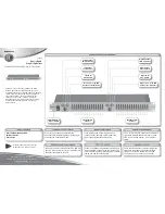
6. SPK PCB
Proceeding :
TOP COVER
→
BACK CHASSIS
→
DIGITAL PCB
→
SIDE CONNECT PCB
→
VIDEO PCB
→
INPUT and HDAM PCB
→
FRONT CONNECT and FUSE PCB
→
SPK PCB
(1) Remove the screws.
(2) Remove the connector wire.
(3) Remove the connector wire. Remove the screws. Then remove the front connector PCB and the fuse PCB.
View from the bottom
CN703
CN704
CN702
CN701
BN932
CN940
CN941
BN933
CN25D
18
Summary of Contents for SR7009/FN
Page 8: ...Personal notes 8 ...
Page 27: ...Personal notes 27 ...
Page 73: ...Personal notes Personal notes 73 ...
Page 201: ...AK5358BET DIGITAL IC306 AK5358BET Pin Function 201 ...
Page 206: ...NJW1194A INPUT IC484 IC489 BLOCK DIAGRAM 206 ...
Page 207: ...2 FL DISPLAY FLD GP1261AI FRONT FL602 PIN CONNECTION PATTERN DETAIL 207 ...


