background image

MAIN (A SIDE)

MAIN (B SIDE)

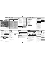
PRINTED CIRCUIT BOARDS

C183

C351

C254

C277

C278

C281

C234

C324 R397

PF103

C132

C155

C192

C346

L122

R338

C122

CP101

Q130

R392

C106

C150

IC

111

Q101

Q104

R102

R117

R119

R128

R139

R196

R202

R320

C103

C140

Q1

10

R143

C1

18

C262

Q129

C1

14

R109

R112

C108

R561

R295

C261

FPC101

FPC104

C220

C189C196

R245R265

C245

R508

C214

C187

C145

R133

R134

C236

Q102

Q105

R140

R197

R203

C105

C265
C273

C293

C260

L1

12

L1

13

R246R268

R281

R282

R289

R290

R445

R308

IC117

C340

C341

C309 C31

1

R145

R493

C129

R371

R377

C182

C350

R555

C172

C241

IC110

R447

R449

R509

C125

C152

D120

IC106

R341 R425

R426

R501

C301

C302

C305

C306

C312

C313

C342

CP103

CP104

C142

C251

C252

C299

C104

C112

R101

R105R486

R488

R492

C102

Q128

C116

PF101

C188

C191C195

CP102

R251R264

R565

FPC103

IC105

JACK105

R476

X101

GND101

C137

JACK102

R104

R106

R121

R135

R487

R489

Q127

CP106

L1

10

L111

R248R267

R279

R280

R287

R288

FPC102

JACK104

2.KEY3

14.D5

16.D3

18.D1

26.EL_RST

28.DGND

34.NC

24.EL_DC

27P

1.RESET

3.TXD 4.RXD

9.KEY2

11.KEY1

13.D7

15.DGND

17.D6

27.EL_CS
23.D0

10P

LB+ LB- GND LA+ LA-

16P

7.DGND

10.DGND

8.D_+12V

5.AGND 4.A_+12V

2.BI_AMP 1.P_DOWN

RB+ RB-

5.DGND 4.D_+12V

RA+ RA-

1.DGND

2.D_+5V

2.AGND

3P

4.TCK

5.MGND

6.MD0

7.MD1

8.EMLE

9.TRST#

10.TDO

21P

1.RESET

6.REMOTE

20.EL_RD

22.DGND

2.CPU_+3V3

19.D4

21.D2

GD25Q32B

7.DSP

 BOOT

MCR51

1:30P

  MCR61

1:34P

MCR51

1 5P

MCR61

1 23P

BKT804

12.NFC_ACK 11.+18V_OLED

9.STBY_+5V

3.POWER_H

12P

3.HP_L

611

511

2.CPU_+3V3

24.576MHz

16.BUS2

17.BUS3
19.MGND

15.BUS1

14.MGND

18.CD_SRAMSTB

8.CD_INSW

9.CD_CLSW

12.CD_CCE

7.CD_DECRST

10.CD_CPSW

11.CD_BUCK

3.CD_OPEN

1.CD_LDCHK

2.CD_CLOSE
4.CD_MSTBY

BD4730

4.CPU_+3V3

10.OLED_+16V

12.OLED_+16V
8.OLED_+3V3

30.I2S_SDA

32.LED_+5V

AZ1117CH-3.3

5.MGND

24.CY920LRCK

25.CY920_MCLK

26.MGND

27.MGND

16.SPI_MIEO

17.SPI_CLK

18.SPI_CS

19.FACT_RST

20.SPI_REQ

21.CY920_DATA/DSDL

9.U_PWR1

10.REAR_USB_SW(OE2)

11.FRONT_USB_SW(OE1)

12.OC_FLAG1

13.OC_FLAG2

14.E_RST

1.USB_OE

2.FET_5V_ON

3.FET_2V2_ON

4.DC/DC_1V8_ON

5.DC/DC_2V5_ON

6.DC/DC_3V3_ON

1.D_+3V3

2.DGND

3.OPT1

5.WPS_ON

4.OPT2

LM7805

8.ST_+5V

9.ST_+5V

16.DGND

11.TU_CLK

12.TU_SDA/DI

13.TU_CE

14.TU_RST

15.TU_INT/DO

20.AGND

22.AGND

19.AIN_CONT

21.L_OUT

23.R_OUT

6.A_-12V

3.DGND

BKT805

GND

10P

6.CD_DREQ

20.SPDIF

5.CD_SBSY

21.MGND

13.BUS0

3.TDI

11.TMS

NJM2387ADL3

R1EX24128BSAS0I

6.CNVSS

22.CY920_DSDR

23.CY920_BCK/DSD_BCK

7.IOS(WIFI)

8.U_PWR2

15.SPI_MOEI

10.TU/DAB_ON

17.A_+5V

18.A_+5V

23P

6.SPDIF

7.DGND

WHITE

BLACK

BLACK

1.HP_R

BLACK

511

RED

611

RING,TER WIRE       MTG

1.LED_RED

3.LED_GREEN

7.LED_OR

25.EL_RW

29.I2S_SCL

31.LED_RST

33.LED_+5V

NJM8068

5.HP_DET

RED

RED

R450

R453

R307

C248

R502

C268

R191

R173

R208

R454 R455

R347

R424

R342

R387

R163

R353 R355 R357

R375

Q123

R433

R431

R298

R314

R316

R322

D111

R127

L1

17

R124

R126

C206

R284

R403

R297

R218

R240

C168

R185

R186

C158 C345

C264

C266

C267

C144

C217

L108

L109

C133

R335 R393 R394

C139

C310

R120

C127

L103

Q1

17

Q1

16

C141

R446

R448

C215

C216

C249

R362

D116

R554

C165

R348

C307

R364

R388

D1

19

R168

R175

R180

R201

R333

R354 R356 R358

R507

C271

C272

C315

R415

R558

C202

C205

D110

R241

R293

C235

C244

R323

C164

R194

C199

R456

Q121

R272

Q118

R158

R161

R547 R548

R152

C135

C148

R149

R472

R310

C179

C160

R179

R474

C110

C121

R220

R330 R332

R360

C134

L107

R325

C322

R395

C253

C276

C275

C

111

R

111

Q126

R324

R114

R329

Q1

12

Q

111

R144

C1

15

C128

R1

13

R564

C221

R477

R490
R491

C123

C291 C292

R118

R129

C107

R103

R441

R442

R443

R451

R452

R300

R302

R309

R317

C287

Q120

R167

R169

C171

C177 C178

C185

Q125

R212

R440

R171

R222

R250

R269 R274

R432

R301

R303

R349 R351

C237

C238

R339

R428

R504

C308

C314

D106

R401

R404

R406

R399

L125

R482

R483

R125

R407

R410

L102

C246

C180

C204

C223

C186

C181

R505 C226

C348

R176

R238

L101

L105

C1

17

R1

15

C256

L126

C230

R369

C240

C239

R334 R337

C282

C154 C263

L119

L120

C131

L127

C337

C338

C339

C318

L1

15

L1

16

R402

R166

C269

Q1

15

Q132

L114

L118

C109

C120

C119

R108

Pb

CLP101

R560

R444

C247

C250

C270

IC114

R566 R567

C286

IC116

R562

R563

C151

L121

R553

R556 R557

R559

D109

R170

R172

R174

R198

R205 R213

R350 R352

R429

R435

R506

C355

IC109

R312

R381

R416

R592R593

R594

X102

R457 R458

R411

Pb

R576

R577

R578

R155

R398

R405

R408

C126

C174

C175

C198

C255

R340

R409

C136

C149

R165 R471

IN

OP

FI

ADJ

ICT

C243

C193

C208

C212

C211

C138

C161

C162

C347

R475

R51

1

R534

C219

C222

C130

R110

R164

R221

R418

R419

R420

PF102

C190

C232

C233

IC108

C143

C356

R421

R522

R470

R469

C295

D101

D103

D121

Q103

R123

R130

R136

C259

D1

15

IC113

R518

R519

FPC106

C166

IC103

R182

R514

C224

C357

C358

IC107

C227

C228

C229

C242

C320

R315

R318

R363

R365

R367

R378

R535

C300

C304

C336

C343

C329
C330

C331

C323

C325

C326

R521

C200

R247

R258

R260R263

R266

R296

R299

Q106

R539

L104

R389

R391

C317

C316

R376

C296

C332

C344

R368

C327

C328

R525
R526

C209

IC104

R278

R283

R285R286

IC102

R527

R528 R529

R530

R531

Q113

D108

C101

C197

C203

C207

R261

R275

R276

R277

R291R292

R305R306

IC101

IC112

7.DGND

10.DGND

6.A_-12V

2.BI_AMP

4.A_+12V

4.MGND

ICS51

1

1.DGND 2D_+12V 3.DGND 4.D_+5V 5.DGND

1.HP_R 2.AGND 3.HP_L

12.NFC_ACK

8.D_+12V 9.STBY_+5V

1.P_DOWN

3.POWER_H

1.CPU_+3V3

2.TXT_232

14.D5

16.D3

10.OLED_+16V

12.OLED_+16V
8.OLED_+3V3

9.KEY2

11.KEY1

13.D7

15.DGND

7.LED_OR

6.REMOTE

5.HP_DET

26.EL_RST

28.DGND

22.DGND

24.EL_DC

30.I2S_SDA

32.LED_+5V

25.EL_RW

27.EL_CS
23.D0

29.I2S_SCL

31.LED_RST

21.D2

20.EL_RD

19.D4

20.SPDIF

21.MGND

19.MGND

18.CD_SRAMSTB

15.BUS1

14.MGND

13.BUS0

12.CD_CCE

11.CD_BUCK

10.CD_CPSW

8.CD_INSW

7.CD_DECRST

6.CD_DREQ

5.CD_SBSY

4.CD_MSTBY

3.CD_OPEN

2.CD_CLOSE

23.CY920_BCK/DSD_BCK

22.CY920_DSDR

21.CY920_DATA/DSDL

20.SPI_REQ

25.CY920_MCLK

24.CY920LRCK

15.SPI_MOEI

14.E_RST

13.OC_FLAG2

12.OC_FLAG1

18.SPI_CS

17.SPI_CLK

16.SPI_MIEO

8.U_PWR2

7.IOS(WIFI)

6.DC/DC_3V3_ON

5.DC/DC_2V5_ON

10.REAR_USB_SW(OE2)

9.U_PWR1

2.FET_5V_ON

1.USB_OE

3.OPT1

4.OPT2

6.SPDIF

7.DGND

2.DGND

5.WPS_ON

11.TU_CLK

13.TU_CE

14.TU_RST

20.AGND

22.AGND

19.AIN_CONT

21.L_OUT

23.R_OUT

18.A_+5V

PCM9211

STA309A

NJM8068

5.AGND

AZ1117CH-3.3

3.RXD_232

2.KEY3

1.LED_RED

4.CPU_+3V3

3.LED_GREEN

18.D1

34.NC

17.D6

33.LED_+5V

17.BUS3

16.BUS2

9.CD_CLSW

4.DC/DC_1V8_ON

3.FET_2V2_ON

11.FRONT_USB_SW(OE1)

19.FACT_RST

27.MGND

26.MGND

1.CD_LDCHK

1.D_+3V3

16.DGND

8.ST_+5V

9.ST_+5V

17.A_+5V

TAS5558DCAR

11.+18V_OLED

NJM4556AM

12.TU_SDA/DI

15.TU_INT/DO

10.TU/DAB_ON

R5F56108VNFP

Q133

Q131

C335

R254

C167

R613

R184

Q107

R141

Q135

Q136

R243

R478

Q124

R204

R495

D114

D105

C184

R253

R242

R244

R494

Q119

C194

R467 R473

R146

R157

R160

R132

R552

R510

R390

R615

R327

Q108

R541

R380

C176

R439

C257

R343

R344

R345

R384

R430

C290

R216

R217

R346

R359

R385

R226

R434

R319

R326

R271

R273

R515 R516

R536

R178 R183

R199

C147

Q114

C159

R181

R192

R195

R396

R400

R150

C353

D112

R235

R262

R413 R414

R479 R480

R500

Q122

R219

Q137

R138

R148

R233 R234

R532

C352

R159

R162

C349

C153

R512

C294

C303

C124

R137

R147

R153

C280

R372

R373

D1

17

D102

R107

R1

16

R122

R131

R177

C213

C225

C231

C274

R331

R336

R361

R374

R379

R417

R370

C319

R311

R313

R459

C284

C333

C334

R383

R224

R236

R591

R589

L129

R544

R545

R546

R151

C354

D118

R499

Q134

D107

Q109

D113

C201

R481 R485

R225

R227

R228

R229

R230

R255

R304

R223

R249 R252 R256

L106

R188

R189

R538 R540

C321

R465 R466

R523

R468

R614

R422

R423

D104

R542 R543

C298

L124

C279
C285

C288
C289

D122

C258

R520

R460

R461

R462

R463

C297

L123

R193

R206

R207

R209

R210

R21

1

R214

R215

R239

R436

R437

R438

C283

R321

R328

R366

R382

R386

R427

R590

C156

L128

C157

R270

R464

R503

R513

R517

R524

C146

R142

R154

R156

R496 R497

R498

C210

R231

R232

R257 R259

R294

R412

R484

C163

C169

C170

C173

R187

R190R200

R237

R533

R537

Lead-free Solder

When soldering, use the Lead-free Solder (Sn-Ag-Cu).

鉛フリー半田

半田付けには、鉛フリー半田 (Sn-Ag-Cu) を使用してください。

51

1

2

3

4

5

6

7

8

9

10

11

12

13

14

15

16

A

B

C

D

E

F

G

H

J

K

L

M

A

B

C

D

E

F

G

H

J

K

L

M

1

2

3

4

5

6

7

8

9

10

11

12

13

14

15

16

Summary of Contents for M-CR611/FN

Page 1: ...the maximum extent possible Ver 4 Some illustrations using in this service manual are slightly different from the actual set Please use this service manual with referring to the operating instruction...

Page 2: ...he laser pick up is defective 19 SPECIAL MODE 20 Special mode setting button 20 1 Factory Initialization Mode 21 2 User Initialization Mode 22 3 Version Display Mode 23 4 CD test mode 25 5 Protection...

Page 3: ...you can do with this manual Search for a Ref No phrase Ctrl Shift F You can use the search function in Acrobat Reader to search for a Ref No in schematic diagrams printed wiring circuit diagrams block...

Page 4: ...Adobe Reader 9 On the Document menu click Sign Magnify schematic printed circuit board diagrams 1 Ctrl Space mouse operation Press Ctrl Space on the keyboard and drag the mouse to select the area you...

Page 5: ...en Example using Adobe Reader 9 On the Tools menu point to Select Zoom and then click Pan Zoom Window Magnify schematic printed circuit board diagrams 3 Loupe Tool function The Loupe Tool function let...

Page 6: ...tant safety parts that are indicated by the z mark on schematic diagrams and parts lists be sure to use the designated parts Be sure to mount parts and arrange the wires as they were originally placed...

Page 7: ...a part make a clear distinction between 1 and I i to avoid mis supplying 3 A part ordered without specifying its part number can not be supplied 4 Part indicated by mark is not illustrated in the expl...

Page 8: ...ential WARNING Safety regulations require that the set be restored to its original condition and that parts which are identical with those specified be used Veiligheidsbepalingen vereisen dat het appa...

Page 9: ...WEP 64bit WEP 128bit WPA WPA2 PSK AES WPA WPA2 PSK TKIP Radio frequency 2 4 GHz No of channels for N K F 1 13ch for U 1 11ch 1 The Wi Fi CERTIFIED Logo and the Wi Fi CERTIFIED On Product Logo are regi...

Page 10: ...10 DIMENSION Unit in mm 5 1 8 130 11 1 2 292 4 3 4 120 4 1 4 105 1 4 6 12 1 8 305 1 7 8 46 1 1 2 38 8 5 8 218 8 3 8 210 1 1 2 35 1 1 2 35 1 1 4 30 1 8 3 Weight 7 lbs 4 oz 3 4 kg...

Page 11: ...then turn the power off s During this time start and initialize the network devices Service tools Measuring Disc CD TCD 784 CD R TCD R082W CD RW TCD W082W z See MEASURING METHOD AND WAVEFORMS Replaci...

Page 12: ...e SMPS PCB wire connector a surge current may flow due to the charge stored in the AMP PCB causing damage to the D AMP IC500 and IC502 2 When attaching the AMP PCB to the MAIN PCB connector insert the...

Page 13: ...SASSEMBLY 8 BACK CHASSIS ASSY and EXPLODED VIEW BACK CHASSIS Ref No of EXPLODED VIEW 52 MECHA SUPPORT L R See DISASSEMBLY 4 MECHA SUPPORT L R and EXPLODED VIEW MECHA SUPPORT L R Ref No of EXPLODED VIE...

Page 14: ...indicate the shooting directions of photos The photographs with no shooting direction indicated were taken from the top of the unit Photos of M CR611 N1B are used in this manual The viewpoint of each...

Page 15: ...e CD tray and remove WINDOWS LOADER 2 Remove the screws 3 Remove the screws Remove the CORD HOLDERs and connector wires Remove the connector wire Shooting direction A Shooting direction D Shooting dir...

Page 16: ...ern for LD damage prevention has been short circuited Be sure to wear an earth band 4 MECHA SUPPORT L R Proceeding PANEL SIDE TOP PANEL FRONT PANEL ASSY CD MECHA ASSY MECHA SUPPORT L R See EXPLODED VI...

Page 17: ...RT L R TUNER SHIELD COVER 1 Remove the screws 7 SMPS PCB Proceeding PANEL SIDE TOP PANEL FRONT PANEL ASSY CD MECHA ASSY MECHA SUPPORT L R TUNER SHIELD COVER SMPS PCB 1 Remove the screws Remove the con...

Page 18: ...NER SHIELD COVER SMPS PCB BACK CHASSIS ASSY 1 Remove the screws 9 MAIN PCB ASSY Proceeding PANEL SIDE TOP COVER FRONT PANEL ASSY CD MECHA ASSY MECHA SUPPORT L R TUNER SHIELD COVER SMPS PCB BACK CHASSI...

Page 19: ...chanism prior to anchoring in the set should be protected against static electricity and dust The mechanism must be stored where abnormal external force is not applied When carrying the finished mecha...

Page 20: ...ry display mode X Displays the protection occurrence history See page 28 7 DPMS forced up date mode X Mode used for development This is not used during servicing 8 Access to development server mode X...

Page 21: ...WPS and iOS buttons when the Standby Indicator lights The unit switches to the factory initialization mode Startup display All indicators light 2 seconds Standby indicator lights green All off 2 seco...

Page 22: ...ection Network devices are started and initialized s 2 1 Operations Press and hold the power operation button X before inserting the power plug then insert the power plug while hold ing down the butto...

Page 23: ...on display Press the Input button and use CURSOR 1 and CURSOR 0 to select press the Enter button the Version within the Setup items 3 3 Display Order q system com Version w system com Boot Loader Vers...

Page 24: ...mage Network u com is displayed When Network Module CY920 startup is incomplete CURSOR f t Serial No MZ_ Fixed characters b Last digit of year cc Week number dddddd Serial number CURSOR f y Bluetooth...

Page 25: ...Test Mode is displayed for 5 seconds CD TEST MODE indicator when disc is loaded Remove the power plug to exit this mode 4 2 Before starting the test Open the tray and set the disc Even when a disc is...

Page 26: ...outer circumference OUT positions for playback and performs the error count 4 4 Pickup movement When CD test mode is ready to start press the CURSOR 1 CURSOR 0 button to move the pickup in FWD outwar...

Page 27: ...FFSET yTRACKING OFFSET uRFRP Caution If you have not completed the adjustment the displayed values are not correct 4 6 Displaying the laser current In CD TEST MODE press and hold the VOLUME d button f...

Page 28: ...ting the count value With the accumulated laser on time displayed press and hold the 1 3 button for over 5 second to reset the count value overwrite the stored data 5 Protection History Display Mode 5...

Page 29: ...e DC protect 1 Power line short circuit 29V D AMP power f DC protect 2 Power line short circuit 12V_D 12V_A 12V 5V Resetting the protection history With the protection history displayed press and hold...

Page 30: ...ROM differing from that of the EXTERNAL ROM In this case see Update Procedure in the Event of a CY920 Error This does not require special operations such as pushing multiple buttons at the same time T...

Page 31: ...t of this unit using a USB cable Do not use an extension cable when connecting the USB unit If a USB memory device cannot be updated replace it with a different USB memory device and perform the updat...

Page 32: ...rt NOTE Remove the LAN cable from this unit when performing updates 1 5 Start the update Press and hold the power operation button before inserting the power plug then insert the power plug while hold...

Page 33: ...g while holding down the button and wait for more than 3 seconds Select USB Update using CURSOR d and CURSOR f then press the Enter button to select 2 4 Forced USB All Device Write Mode The following...

Page 34: ...Update 3 Press the ENTER button The latest version of the firmware uploaded to the web is displayed If the latest firmware version is on the web proceed to 4 If the latest firmware is already install...

Page 35: ...isition recived error Main rewirte Firmware recived data incorrect Check Sum Error Updating fail 12 13 Rewrite failure Block Erase failued before Main rewriting Erase fail 13 14 Rewrite failure Block...

Page 36: ...the voltages of pins within CN221 other than those listed above are only output when the power is ON Check Power Supply Voltages for System com MAIN PCB STBY 5 V CP103 9 pin Check Drive Signals for OL...

Page 37: ...no faults in the IC500 or IC502 TAS5142 if an approx 29VP P square wave is confirmed at each terminal No faults Identify the input function from which sound is not output or from which noise occurs an...

Page 38: ...eform MAIN PCB IC108 11 pin MCLK MCLK OK Check Soldering or replace for the following parts IC110 IN 12V_A OUT 5V_A IC113 IN ST 5V OUT 3V_D1 MAIN PCB Check Soldering or replace for the following parts...

Page 39: ...12 86 87 88 89 pin IC107 23 24 25 26 pin DIR_DO DIR_DI DIR_CLK DIR_CE NG OK Check control signal for PWM CONTROLLER MAIN PCB IC108 20 21 pin SDA SCL IC108 18 14pin PDN MUTE Hi level O K END Check Sold...

Page 40: ...Input for CODEC MAIN PCB IC107 30 pin CD_SPDIF OK OK OK OK OK 2 3 CD playback END Check Soldering or replace for the following parts CD PCB CN703 IC705 IC704 SMPS PCB IC441 Check Soldering or replace...

Page 41: ...he DIR input IC107 32 pin OK OK OK OK OK OK OK Check Soldering or replace for the following parts IC110 IN 12V_A OUT 5V_A on MAIN PCB CP106 17 pin A 5V on MAIN PCB Check Soldering or replace for the f...

Page 42: ...ring or replace for the following parts JK810 JK811 1pin for the OPTICAL PCB NG NG to 2 1 COMMON signal 2 5 Analog In 1 Check Analog Audio Signal from Analog1 INPUT PCB JK2 L R ALL Model Area C75 C82...

Page 43: ...P813 21 pin CY920_DATA DSDL OK OK OK OK OK Check Soldering or replace for the following parts Network PCB CP805 1 2 3 pin NET_5V CN223 1 2 3 pin NET_5V SMPS PCB Check Soldering or replace for the foll...

Page 44: ...sure the voltage for the points above is Lo level O K Replace each device MAIN PCB Q106 Q107 Q113 Q114 OK OK OK OK OK Check Soldering or replace for the following parts MAIN PCB IC102 3 12 44 52 59 30...

Page 45: ..._USB_SW OE2 9 U_PWR1 2 FET_5V_ON 1 USB_OE 3 OPT1 4 OPT2 6 SPDIF 7 DGND 2 DGND 5 WPS_ON 11 TU_CLK 13 TU_CE 14 TU_RST 20 AGND 22 AGND 19 AIN_CONT 21 L_OUT 23 R_OUT 18 A_ 5V PCM9211 STA309A NJM8068 5 AGN...

Page 46: ...PLAY qRFEQO wRFO eFEI rFOO tTEI yTRO uFMO iDMO 1V div 500mV div 1V div 1V div 1V div 500mV div 1V div 1V div 500mV div 1V div 1V div 1V div 500mV div 1V div 1V div 500mV div qRFEQO 1 3 CD RW TCDW082W...

Page 47: ...4 CD Playback 5 LOADER OPEN CLOSE Q3LRCK Q4SCLK Q5SDATA STANDARD GND STANDARD GND B C oOPSW Q0FCLSW Q2LOAD Q1LOAD OPEN CLOSE 47...

Page 48: ...NLY TUNER BT ANT LAN USB REAR WPS D D FRONT USB PCB NFC ANT PCB INPUT_SEL MFI USB_OE OC_FLAG1 OC_FLAG2 U_PWR1 FUSB_SW FACT_RST SPI_CLK SPI_MOEI TLC59108 R G SLED TC94A92FG CD_SDRAMSTB EL_RW EL_CS I2C...

Page 49: ...ICK_UP OPTICAL PCM9211 PWM_CONTROL GD25Q32B R1EX24128BSAS0I RESET_IC MICOM NKM2068 NJM4556 OPAMP DGND 20V HGND KIA79L12 12V_LDO TPS54340 12V_D FET SWITCH ST_BY_0 3W TAGET_0 2W BD82065FVJ BD82065FVJ VB...

Page 50: ...R511 6PWAFER 5P WAFER 10P BD TO BD MCR611 6P BD TO BD MCR511 Verona2 5P PATTERN MCR611 ONLY LED L 33P FFC MCR611 29P FFC MCR511 29P FFC MCR511 33P FFC MCR611 33P FFC MCR611 33P FFC MCR611 29P FFC MCR5...

Page 51: ...54 C263 L119 L120 C131 L127 C337 C338 C339 C318 L115 L116 R402 R166 C269 Q115 Q132 L114 L118 C109 C120 C119 R108 Pb CLP101 R 5 6 0 R444 C247 C250 C270 IC114 R566 R567 C286 IC116 R562 R563 C151 L121 R5...

Page 52: ...15 DGND 10 16V 8 3V3_D1 9 KEY2 7 LED_OR 2 KEY3 CP6 13 D7 16 D3 17 D6 18 D1 19 D4 23 D0 11 KEY1 17 D6 12 16V 5 H P_DET 1 LED_RED 4 3V3_CPU 5 H P_DET 6 REMOTE 7 LED_OR 10 16V 11 KEY1 12 16V 22 DGND 24 E...

Page 53: ...25 FPC1 R31 R32 C11 R5 C33 C40 C51 L1 C56 C57 R1 R2 C14 C6 R8 C10 R4 GND12 FPC2 Q1 JK1 2 KEY3 1 KEY2 3 DGND 7 D6 6 D7 5 CLS 8 D5 11 D2 24 NC FPC1 33P 4 3V3_CPU 5 H P_DET 3 LED_GREEN 6 REMOTE 11 KEY1 9...

Page 54: ...910 CP811 C803 CP805 R568 R569 R570 C929 C930 CN802 CN807 CP809 SW800 SW801 CN801 CP813 INT EXT CY920 D D BD11600NUX 1 VBUS 2 D HOLE 6P 27P VBUS GND BD11600NUX BKT800 M3 BRACKET 1 NET_5V 2 NET_5V 3 NE...

Page 55: ...L 10 AGND 11 DAB_R 2 DGND 3 5V 4 5V 5 DAB_ON 1 DAB_SPDIF R809 R812 R822 C807 C809 R825 C812 C810 R808 C820 C822 R815 R819 C813 C811 C943 R939 JK811 CP812 Pb BKT901 R941 R940 C945 1 OPT2 2 DGND 3 OPT1...

Page 56: ...7 DGND 10K R128 11 TU_CLK 13 TU_CE 15 TU_INT DO 9 ST 5V 220 10 C241 C187 220 6 3 17 A 5V 19 AIN_CONT 21 L_OUT KRC107S Q127 CLZ9R001Z CBW160808U121T R202 47 L109 BD121 R220 0 4K7 R279 R280 4K7 C144 100...

Page 57: ...3V R851 348K C834 22UF 6 3V CP805 64 62 58 54 52 48 44 38 34 30 28 24 20 18 14 10 6 8 4 60 50 46 56 40 36 42 32 26 22 16 12 2 63 61 57 53 51 47 43 41 37 33 27 23 19 17 13 9 7 3 59 49 55 45 39 35 31 2...

Page 58: ...CP804 TO NETWORK PCB C956 10P C951 0 1608 R946 R947 1 3 2 JK810 C954 0 1608 R944 0 SW914 C946 100N R943 0 SW913 100 6 3 C843 TO CNT PCB CP821 5P_WAFER PWM3 SPDIF SPI_CLK MFIO22 DAB_TX_M_RX POR_N R805...

Page 59: ...RESET GND_D I2C_SDA LED_RST CH_GND C88 0 C85 0 C77 0 C70 1N K C67 100N K CP6 MCR511 30P MCR611 34P LED_RED LED_GREEN H P DET LED_OR D7 KEY2_1 KEY1_1 GND_D EL_RD EL_RD GND_D EL_D C EL_RESET GND_D EL_D...

Page 60: ...8 1R5 2 0mm WIRE DGND C958 100N K C956 18P J NFC ANTTENA FROM NETWORK PCB 2 1 CN910 2P WIRE NFC_INTRP NFC 1 4 2 3 IC901 NTAG203F SCHEMATIC DIAGRAMS 5 10 SCH05_NFC 60 1 2 3 4 5 6 7 8 9 10 11 12 13 14 1...

Page 61: ...12 10uH L510 10uH 4700 M C584 L502 10uH L504 10uH C583 47N C568 47N 51K R580 R589 C579 C597 10N C550 100N CN500 FROM SMPS UNIT C557 1000N C555 1000N C558 1000N R574 0 C540 100N C589 33N 20 C565 33N 20...

Page 62: ...RC102S DGND 47 16 5 7 C36 DGND LED1 WEJ3290W R10 120 R26 R27 C2 10N K C3 1N K C1 100N K 16V_OLED LED_RED LED_GREEN R51 0 3V3_D1 REMOTE 16V_OLED H P_DET RW WR D1_SDIN 16V_OLED EL_CS C27 47P J R48 1M EL...

Page 63: ...SPDIF DAB_OUT DAB_ON D 5V DAB_R DAB_L INPUT SW9 CURSOR UP SW3 R22 3K3 R16 10K SW10 R14 1K8 SW4 R23 2K7 R24 3K9 SW12 R17 6K8 SW8 R15 2K7 SW6 SKIP REV R25 6K8 SW13 CH_GND DGND SW2 C54 1N K C43 10N K C5...

Page 64: ...1504S CD_CCE CD_CLSW CD_DECRST CD_SBSY CD_OPEN CD_LDCHK D701 1SS355 470 16V C779 C781 0 1 GND_DA C728 0 1 C724 0 1 10K R744 GND_DA GND_DA R789 10K R786 10K AGND A 3 3V C771 5600P 0 R764 C772 0 047u C7...

Page 65: ...C875 0 22J 2012 C875 0 22J 2012 1 2 R426 86 6KF 2012 R426 86 6KF 2012 C413 104K 2012 C413 104K 2012 R812 120K 3216 R812 120K 3216 D876 UZ22B D876 UZ22B 1 2 C871 103K 630V MPE C871 103K 630V MPE 1 2 L4...

Page 66: ...43 42 40 44 45 41 48 50 38 39 46 51 25 26 RD RD BK BK 41 62 5 63 S5 2 U F K S10 2 S9 4 S8 4 S9 4 S4 1 S2 12 S11 4 S11 4 S11 4 64 64 65 66 S3 2 S1 9 S5 2 S12 4 S7 4 S7 1 S7 2 S7 1 S7 1 S6 4 S6 6 S7 3 S...

Page 67: ...1 SET FRONT C D 1 7 6 5 2 9 10 11 12 13 14 8 8 Adhesive 39 8 15 17 16 37 4 3 18 19 C D 23 14 21 20 22 19 26 25 27 28 29 22 20 30 19 23 C D 23 21 20 22 19 24 29 22 20 31 19 23 26 20 25 32 32 26 20 25 3...

Page 68: ...Only major semiconductors are shown general semiconductors etc are omitted to list The semiconductor which described a detailed drawing in a schematic diagram are omitted to list 1 IC s R5F56108VNFP...

Page 69: ...L O L O O EL Writing 29 EL CS O O L O L O L O L O L EL Chip Select L I F communication 30 D7 O O L O L I O O Data Bus for OLED 31 D6 O O L O L I O O Data Bus for OLED 32 D5 O O L O L I O O Data Bus f...

Page 70: ...O L O L O L O L PCM9211 DIR Control 89 DIR_CE O O L O L O L O L O L PCM9211 DIR Control 90 DIR_RERR PD I I I I I I PCM9211 DIR Control 91 VCC 3 3V_CPU 92 TEST3 PD I I I I I I Boot for Check PCB mode...

Page 71: ...H DM870 VBUS Control 127 TEST4 PD I I I I I I Boot for Check PCB mode 128 LED_ORANGE PD O O L O H O L O L O L Control ORANGE Red Green LED 129 LED_RED PD O O L O L O H O L O H Control RED LED 130 VSS...

Page 72: ...ET RFDC VREF PVREF TNi TPi FPi1 FPi2 FNi1 FNi2 TRo DMo FMo Foo FSMoNiT FEi SBAD RFDC 10bit ADC MDi LDo RFEQo AGCi RF Ripple DET RFRP RFRPi VRo RFRP RFRP SBAD RFDC FEI TEI Reference Voltage APC Bias ci...

Page 73: ...IN diode B I 15 TPi I 3AI F Sub beam signal input pin To be connected to PIN diode F I 16 TNi I 3AI F Sub beam signal input pin To be connected to PIN diode E I 17 VRo O 3AI F 1 65 V reference voltage...

Page 74: ...46 DVSS3L Grounding pin for 3 3V Muiti Bit DAC Circuit 47 XVSS3 Grounding pin for 3 3V clock oscillator circuit 48 Xi I 3AI F System clock Input pin I Xtal oscillation circuit Connect feedback resist...

Page 75: ...2 Pin Assinment Table 69 RST I 3I F Reset Input pin I Schmitt input 70 Test I 3I F Test pin L fixed I Connect to GND for normal operation 71 VDD1 1 Power Supply pin for 1 5V Digital circuit 72 VSS 1 G...

Page 76: ...TR Built in mute circuit Built in Tray motor speed control circuit Wide operating supply voltage range 6 5V 13 2V Device Package Operating Temp IP4001 28SSOPH 375 35OC 85OC IP4001TF 28SSOPH 375 35OC 8...

Page 77: ...orporated Submit Documentation Feedback 7 Product Folder Link s PCM9211 Clock Data Recovery MPIO_A SELECTOR MPIO_C SELECTOR MPIO _B SELECTOR ADC Com Supply MPO0 1 SELECTOR MPO 0 MPO 1 MAIN OUTPUT SCKO...

Page 78: ...I Yes Software control I F SPI chip select I2C slave address setting1 2 27 MODE I No Control mode setting see the Serial Control Mode section Control Mode Pin Setting 28 RXIN7 ADIN0 I Yes Biphase sign...

Page 79: ...963 3 1 1R 6623 3 1 1R 7963 3 1 1R 6623 287 FK 9UHI 1 FK 1 FK 9 1 1 1 FK 1 FK 17 287 FK 1 NJM2755 NJM2753 SSOP14 TVSP10 6 9 8 7 10 1 2 3 4 5 GND OUTB IN2A IN1B IN2B Vref V IN1A OUTA CNT1 1 2 3 4 5 6 7...

Page 80: ...ND_C 24 30 P Power ground for half bridge C GND_D 23 29 P Power ground for half bridge D GVDD_A 36 44 P Gate drive voltage supply requires 0 1 F capacitor to AGND GVDD_B 1 1 P Gate drive voltage suppl...

Page 81: ...I O Logic PWM_C OUT_C GND_C PVDD_C BST_C Timing Gate Drive Ctrl PWM Rcv GVDD_C PWM_B OUT_B GND_B PVDD_B BST_B Timing Gate Drive Ctrl PWM Rcv GVDD_B PWM_A OUT_A GND_A PVDD_A BST_A Timing Gate Drive Ctr...

Page 82: ...MO1 15 DO Energy Manger Output interrupt Asserted high when threshold is exceeded HP_SEL 17 DI 5 V Pullup Headphone speaker selector When a logic low is applied the headphone is selected speakers are...

Page 83: ...to prevent electrostatic damage to the MOS gates 1 4 Block Diagram Figure 1 1 Functional Block Diagram 1 5 DESCRIPTION Continued The TAS5558 can drive eight channels of H bridge power stages Texas In...

Page 84: ...al ground or voltage Failure to follow this guideline may result in device damage 2 3 8 9 PGND Input and output power ground Connect these pins to the ground electrode of the input and output filter c...

Page 85: ...O3 pin of 16SOP c 7 REV 1 2 AUG 09 2013 FIGURATIONS 4 PIN DESCRIPTION SYMBOL DESCRIPTION Chip Select SI SIO0 Serial Data Input for 1 x I O Serial Data Input Output for 2xI O or 4xI O read mode SO SIO1...

Page 86: ...kage Dimensions 1 2 3 4 5 6 7 8 9 10 D D 2D 2D GND OE D D S VCC Fig 7 Block diagram Fig 8 Pin configuration Fig 9 Package Dimensions B D 1 1 6 0 0 N LOT No Technical Note BD11600NUX Pin Description Pi...

Page 87: ...er temperature conditions OUT 6 7 8 Power switch output connect to load PowerPAD PAD Internally connected to GND Connect PAD to GND plane as a heatsink for the best thermal performance DGN ONLY PAD ma...

Page 88: ...shold voltage around 4 2 V for more than 55ms 3 CS Input to the comparator of the over current protection A resistor senses the switching current and the resulting voltage is applied to this pin for t...

Page 89: ...s resistor inserted in the source integrated CoolMOS If voltage in CS pin reac internal threshold of the Current Limit Compara Driver output is immediately switched off Furth the current information i...

Page 90: ...6 O GND 7 SW 8 I MOSFET 9 GND BOOT SW MOSFET PWM 1 2V 2 PLL PLL GND 7 COMP 6 FB 5 SW 8 2 3 4 1 VIN EN RT CLK BOOT Thermal Pad 9 HSOIC PACKAGE TOP VIEW Error Amplifier Boot Charge Boot UVLO UVLO Curren...

Page 91: ...of flexible printed circuits FPC are available to meet customers requirements Wide variety of color options are available Custom models are also available by customers requirements 2011 6 This product...

Page 92: ...put channel 3 10 5 V tolerant TTL input buffer LRCKI DSD_2 Input left right clock DSD input channel 2 11 5 V tolerant TTL input buffer BICKI DSD_1 Input serial clock DSD input channel 1 15 5 V toleran...

Page 93: ...channel 3 output B 43 3 3 V capable TTL 16mA output buffer OUT3A PWM channel 3 output A 47 3 3 V capable TTL 16mA output buffer OUT2B PWM channel 2 output B 48 3 3 V capable TTL 16mA output buffer OU...

Page 94: ...D2730460905 SEMI CHIP TR NPN 2SC KTC2875B MB 0 15W LOW ON RES SOT23 RTK REEL J5222875B0010S 2 Q115 119 00D2690192902 SEMI CHIP TR NPN 2SC KRC102S NB 0 2W SOT 23 REEL J522010200210S 5 Q120 963222500350...

Page 95: ...R CHIP THICK 0 J 1 16W 1005REEL C20000006M101S 1 R284 nsp R CHIP THICK 10K J 1 16W 1005REEL C20001036M111S 1 R285 286 nsp R CHIP THICK 0 J 1 16W 1005REEL C20000006M101S 2 R287 290 nsp R CHIP THICK 4...

Page 96: ...P THICK 10K J 1 16W 1608REEL C20001036M160S 3 R460 464 nsp R CHIP THICK 10K J 1 16W 1005REEL C20001036M111S 5 R465 469 nsp R CHIP THICK 0 J 1 16W 1005REEL C20000006M101S 5 R470 nsp R CHIP THICK 220 J...

Page 97: ...L C20001016M101S 2 R890 nsp R NETWORK A TYPE 0J 4 1 16W SMD 1005 C180000040500S 1 R891 nsp R CHIP THICK 100 J 1 16W 1005REEL C20001016M101S 1 R892 nsp R CHIP THICK 10K J 1 16W 1005REEL C20001036M111S...

Page 98: ...101S 1 C232 233 nsp C CERAMIC CHIP HIK X7R 0 1UF K 50V 1608REEL D011104577160S 2 C234 nsp C ELECT CHIP GE 220UF M 6 3V 6 3 5 7 REEL F60 BXJ SY D050221081250S 1 C235 nsp C CERAMIC CHIP HIK X7R 0 1UF K...

Page 99: ...J 1 16W 1608REEL C20002236M160S 1 C843 nsp C ELECT CHIP GE 100UF MVG 6 3V 5 3 5 9 5 3 3REEL Z8156 SY D050101081650S 1 C844 nsp C CERAMIC CHIP HIK X7R 1UF K 10V 1005REEL D011105772101S 1 C845 nsp C CE...

Page 100: ...TER BOARD SCREW 4P SJ4001S A022 00A100B GOLD BKBKRDRD G6124001SA22JS 1 JACK105 963643103270S TER RCA 3PIN RCA 303D 00 10 BK RD WH G606303D0010YS 1 JACK800 963643100130S JACK MODULAR RJ45 1 1W TRANSFOR...

Page 101: ...0 1UF K 50V 1608REEL D011104577160S 1 C31 nsp C CERAMIC CHIP T C X7R 0 01UF K 50V 1608REEL D010103777160S 1 C32 nsp C CERAMIC CHIP T C COG 47PF J 50V 1608REEL D010470167160S 1 C33 35 nsp C CERAMIC CH...

Page 102: ...sp C CERAMIC CHIP HIK X7R 1UF K 25V 1608REEL D011105774161S 1 C530 nsp C CERAMIC CHIP T C CH 0 1UF J 50V 3216REEL GRM31C2C1H104JA01L D010104167303S 1 C531 nsp C CERAMIC CHIP T C C0G 330PF J 100V 1608R...

Page 103: ...943115100330M COIL INDUCTOR POWER INDUCTOR 7G14T 100M RM SAGAMI D310701431010S 4 L514 515 nsp COIL BEAD CBW201209U121T 120ohm SMD2012 TYPE D340201221210S 2 PF101_A 102 nsp CN WAFER 2 5MM FHS285 10 10P...

Page 104: ...p C CERAMIC CHIP HIK X7R 0 1UF K 50V 1608REEL D011104577160S 1 C708 nsp C CERAMIC CHIP HIK X7R0 01UF K 50V 1608REEL D011103777160S 1 C710 nsp C ELECT GE 85C 100UF M 10V 6 3 5 5RE SY Pb Free SY D040101...

Page 105: ...K 50V 1608REEL D011103777160S 1 C818 nsp C CERAMIC CHIP HIK X7R 0 1UF K 50V 1608REEL D011104577160S 1 C819 nsp C CERAMIC CHIP HIK X7R0 01UF K 50V 1608REEL D011103777160S 1 OTHER PARTS GROUP CN701 nsp...

Page 106: ...UF K 50V 1608REEL D011103777160S 1 C59 nsp C CERAMIC CHIP HIK X7R 0 1UF K 50V 1608REEL D011104577160S 1 C60 nsp C CERAMIC CHIP HIK X7R 1000PF K 50V 1608REEL D011102777160S 1 C62 63 nsp C ELECT GE 85C...

Page 107: ...odel F Japan model B Black model SG Silver Gold model GN Green model REF No Part No Part Name Remarks Q ty New Ver SEMICONDUCTORS GROUP IC901 nsp IC LINEAR RF NTAG203F NT2H0301F0DTL HXSON4 J1240203010...

Page 108: ...P HIK X7R 1000PF K 50V 1608REEL D011102777160S 1 C72 nsp C CERAMIC CHIP HIK X7R 0 1UF K 50V 1608REEL D011104577160S 1 C73 nsp C CERAMIC CHIP HIK X7R0 01UF K 50V 1608REEL D011103777160S 1 C74 nsp R CHI...

Page 109: ...L UP ASSY U N K 5098215608030S CGK1A177ZA 1 15 943411102660M BUTTON ASSY MCR611F DENON SG VOL UP ASSY F 5098215608050S CGK1A177WA 1 16 943411102590M BUTTON ASSY MCR611N1GN DENON OPEN U N K 50982155680...

Page 110: ...2410040353010S 4 67 nsp TAPE MCR611N1GN DENON 10 220 0 25T A4 ACETATE 1220212059000S 2 68 nsp TAPE MCR611N1GN DENON 20 30 0 03T AL TAPE W NITTO5000N 1220212069000S 5 69 nsp COVER MCR611N1GN DENON PC S...

Page 111: ...BC FLUTE N 6007213110000S 1 15 963531105250S BOX GIFT MCR611F DENON MCR611 F OFFSET BC FLUTE F 6007213110030S 1 15 963531105240S BOX GIFT MCR611 K OFFSET BC FLUTE K 6007213110020S 1 16 nsp LABEL MCR51...

Reviews: