WAVEFORMS
T8200WF
1-11-1
1DIV: 0.5V 20
µ
s
IC1001 Pin 1
WF1
1DIV: 0.5V 20
µ
s
IC1201 Pin 14
WF2
1DIV: 0.5V 5
µ
s
IC1001 Pin 9
WF6
1DIV: 200V 20
µ
s
CN1571 Pin 1
WF9
1DIV: 5V 20
µ
s
CL1501 Pin 1
WF10
1DIV: 1V 5ms
IC1551 Pin 7
WF11
1DIV: 10V 5ms
CN1571 Pin 4
WF12
1DIV: 20V 20
µ
s
Q2521 Collector
WF14
1DIV: 0.2V 20
µ
s
CN1102 Pin 7
WF18
1DIV: 2V 20
µ
s
Q2511 Base
WF3
1DIV: 2V 20
µ
s
Q2521 Base
WF4
1DIV: 2V 20
µ
s
Q2531 Base
WF5
1DIV: 10V 20
µ
s
Q1572 Collector
WF7
1DIV: 5V 20
µ
s
Q1571 Base
WF8
1DIV: 20V 20
µ
s
Q2531 Collector
WF13
1DIV: 0.2V 20
µ
s
CN1102 Pin 6
WF17
1DIV: 20V 20
µ
s
Q2511 Collector
WF15
1DIV: 1V
0.5ms
CN1102 Pin 10
WF19
1DIV: 0.1V 20
µ
s
TU1001 Pin 5
WF16
Input:
NTSC Color Bar Signal (with 1kHz Audio Signal) --- WF1~WF16
DVD Video (Power on (Stop) MODE) --- WF17, WF18
CD (1KHz Play) --- WF19, WF20
INITIAL POSITION:
Unplug unit from AC outlet for at least five minutes,
reconnect to AC outlet and then turn power on.
(Brightness---Center Color---Center Tint --- Center Contrast---Approx 70%)
Summary of Contents for CMWC13D6
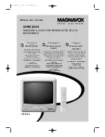
Page 1: ...SERVICE MANUAL 13 COLOR TV DVD CMWC13D6...
Page 38: ...1 10 3 Main 1 4 Schematic Diagram TV Section T8203SCM1...
Page 39: ...1 10 4 T8203SCM2 Main 2 4 Junction Schematic Diagram TV Section...
Page 40: ...1 10 5 T8203SCM3 Main 3 4 CRT Schematic Diagram TV Section...
Page 42: ...1 10 7 Sub Schematic Diagram TV Section T8203SCSUB...
Page 43: ...1 10 8 T8203SCD1 DVD Main 1 3 Schematic Diagram DVD Section...
Page 44: ...1 10 9 T8203SCD2 DVD Main 2 3 Schematic Diagram DVD Section...
Page 45: ...1 10 10 T8203SCD3 DVD Main 3 3 Schematic Diagram DVD Section...
Page 57: ...1 16 2 T8203PEX Packing S1 FRONT X3 X2 TAPE X1 S4 Packing Tape Packing Tape S6 S3 S2 S5...
Page 64: ...CMWC13D6 T8203CD 2006 07 03...