1-4-1
TVDVDN_SN
STANDARD NOTES FOR SERVICING
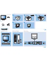
Circuit Board Indications
1. The output pin of the 3 pin Regulator ICs is
indicated as shown.
2. For other ICs, pin 1 and every fifth pin are
indicated as shown.
3. The 1st pin of every male connector is indicated as
shown.
Instructions for Connectors
1. When you connect or disconnect the FFC (Flexible
Foil Connector) cable, be sure to first disconnect
the AC cord.
2. FFC (Flexible Foil Connector) cable should be
inserted parallel into the connector, not at an
angle.
Pb (Lead) Free Solder
Pb free mark will be found on PCBs which use Pb
free solder. (Refer to figure.) For PCBs with Pb free
mark, be sure to use Pb free solder. For PCBs
without Pb free mark, use standard solder.
How to Remove / Install Flat Pack-IC
1. Removal
With Hot-Air Flat Pack-IC Desoldering Machine:
1. Prepare the hot-air flat pack-IC desoldering
machine, then apply hot air to the Flat Pack-IC
(about 5 to 6 seconds). (Fig. S-1-1)
2. Remove the flat pack-IC with tweezers while
applying the hot air.
3. Bottom of the flat pack-IC is fixed with glue to the
CBA; when removing entire flat pack-IC, first apply
soldering iron to center of the flat pack-IC and heat
up. Then remove (glue will be melted). (Fig. S-1-6)
4. Release the flat pack-IC from the CBA using
tweezers. (Fig. S-1-6)
CAUTION:
1. The Flat Pack-IC shape may differ by models. Use
an appropriate hot-air flat pack-IC desoldering
machine, whose shape matches that of the Flat
Pack-IC.
2. Do not supply hot air to the chip parts around the
flat pack-IC for over 6 seconds because damage
to the chip parts may occur. Put masking tape
Top View
Out
In
Bottom View
Input
5
10
Pin 1
Pin 1
FFC Cable
Connector
CBA
* Be careful to avoid a short circuit.
Pb free mark
Fig. S-1-1
Summary of Contents for CMWC13D6
Page 1: ...SERVICE MANUAL 13 COLOR TV DVD CMWC13D6...
Page 38: ...1 10 3 Main 1 4 Schematic Diagram TV Section T8203SCM1...
Page 39: ...1 10 4 T8203SCM2 Main 2 4 Junction Schematic Diagram TV Section...
Page 40: ...1 10 5 T8203SCM3 Main 3 4 CRT Schematic Diagram TV Section...
Page 42: ...1 10 7 Sub Schematic Diagram TV Section T8203SCSUB...
Page 43: ...1 10 8 T8203SCD1 DVD Main 1 3 Schematic Diagram DVD Section...
Page 44: ...1 10 9 T8203SCD2 DVD Main 2 3 Schematic Diagram DVD Section...
Page 45: ...1 10 10 T8203SCD3 DVD Main 3 3 Schematic Diagram DVD Section...
Page 57: ...1 16 2 T8203PEX Packing S1 FRONT X3 X2 TAPE X1 S4 Packing Tape Packing Tape S6 S3 S2 S5...
Page 64: ...CMWC13D6 T8203CD 2006 07 03...