background image

R9MWTU

5-2-55, Minamitsumori, Nishinari-ku, Osaka 557-0063 JAPAN
Phone: +81(6)6659-8201  Fax: +81(6)6659-8510  E-mail: [email protected]

EM-6221  Rev.9  P. 2 / 20

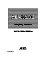
COMPONENT IDENTIFICATION

Terminal Block, Current Input 2

SD Card Slot

PC Configurator Connection Jack

Status Indicator LED

Terminal Block, Current Input 1


FRONT VIEW

Operating Mode Setting DIP SW (SW1)

Terminal Block, 
Voltage Input / Auxiliary Power Supply

T1 3K

T2 3L

17

18

8

9

1K 3K

1L 3L

15

16

6

7

1K 3K

1L 3L

13

14

4

5

1K 3K

1L

3L

11

12

2

3

1K

1L

10

1

8ch

7ch

8ch

6ch

7ch

5ch

6ch

5ch

8ch

7ch

8ch

6ch

7ch

5ch

6ch

5ch

NC 1L

NC 1K

2

1

11

10

3L 1L

3K 1K

4

3

13

12

3L 1L

3K 1K

6

5

15

14

3L 1L

3K 1K

8

7

17

16

3L

3K

9

18

P1

4

U

(

+

)

V

(-)

P2 P3

2

1

6

5

FE1

N

3

7

1ch

2ch

1ch

3ch

2ch

4ch

3ch

4ch

1ch

2ch

1ch

3ch

2ch

4ch

3ch

4ch

7

DB

SLD

DG

NC

NC

2

3

5

6

FE

DA

1

4

Term on

Modbus Terminals

Node Address Setting Rotary SW

Baud Rate Setting Rotary SW

Terminating Resistor SW


STATUS INDICATOR LED

ID

COLOR

STATE

FUNCTION

SDCard

Red

Blinking 

approx. 1 Hz

The unit is preparing to write.
The LED starts blinking 30 seconds before the unit starts writing in the SD card on 
the hour every hour.
DO NOT extract the card while the LED shows the blinking pattern until the writing 
is complete.

2 sec.

SD card access error.
The unit is unable to normally write in the card because it is full or its data contents 
are damaged.

2 sec.

SD card partial access error.
The unit was unable to write in the card for unknown reason but now is recovered.  A 
part of the data contents is missing.

OFF

SD card not inserted.

ON

SD card inserted.

Blinking

approx. 2 Hz

The unit is writing in the SD card.
DO NOT extract the card.

Power

Red

ON

Normal

Blinking

approx. 0.5 Hz

Input overload or no input

Blinking 

approx. 2 Hz

Setting error or device error

2 sec.

Internal calendar error or calendar backup battery life expired.
Re-set the calendar with the PC Configurator.
The LED blinks in the designated pattern every time when the power is turned on 
after the battery life has been expired.

OFF

Device error

RUN

Red

ON

Normal communication

ERR

Red

ON

Received data error

SD

Red

ON

Data transmitting

RD

Red

ON

Data receiving


TERMINATING RESISTOR

To use the terminating resistor, turn the switch ON.


NODE ADDRESS

Node Address is selected between 1 and 99 in decimal.  The 
left switch determines the tenth place digit, while the right 
switch does the ones place digit of the address.

5

4

3

2

1

0

9

8

7

6

5

4

3

2

1

0

9

8

7

6

Node Address Setting (x1)

Factory setting : 00

Node Address Setting (x10)


BAUD RATE

Baud Rate is selected with the rotary switch (4 through 9 
are not available, be sure to set between 0 and 3).

5

4

3

2

1

0

9

8

7

6

Baud Rate Setting

0 : 38.4 kbps (factory setting)
1 : 19.2 kbps
2 : 9600 bps
3 : 4800 bps

Summary of Contents for R9MWTU

Page 1: ...observe these re quirements may invalidate the CE conformance The actual installation environments such as panel con figurations connected devices connected wires may af fect the protection level of this unit when it is integrated in a panel system The user may have to review the CE requirements in regard to the whole system and employ additional protective measures to ensure the CE conform ity In...

Page 2: ... unit is unable to normally write in the card because it is full or its data contents are damaged 2 sec SD card partial access error The unit was unable to write in the card for unknown reason but now is recovered A part of the data contents is missing OFF SD card not inserted ON SD card inserted Blinking approx 2 Hz The unit is writing in the SD card DO NOT extract the card Power Red ON Normal Bl...

Page 3: ...nput 1K 2 5ch 3L Ch 5 Current input 3L 11 5ch 3K Ch 5 Current input 3K 3 6ch 1L Ch 6 Current input 1L 12 6ch 1K Ch 6 Current input 1K 4 6ch 3L Ch 6 Current input 3L 13 6ch 3K Ch 6 Current input 3K 5 7ch 1L Ch 7 Current input 1L 14 7ch 1K Ch 7 Current input 1K 6 7ch 3L Ch 7 Current input 3L 15 7ch 3K Ch 7 Current input 3K 7 8ch 1L Ch 8 Current input 1L 16 8ch 1K Ch 8 Current input 1K 8 8ch 3L Ch 8 ...

Page 4: ...ueezing the latches as shown in the figure below push push DIN RAIL MOUNTING Set the unit so that the lower mounting adaptors are at the bottom Hook the upper hook at the rear side of the unit onto the DIN rail and push in the lower part of the unit When removing the unit pull out the unit while pushing down the adaptors using a minus screwdriver DIN Rail 35 mm wide Mounting Adaptor TERMINAL CONNE...

Page 5: ...rminal 5 6 4 7 8 9 To other Modbus devices 1L 4 P1 5 6 7 P2 P3 N 11 1K 13 14 12 3K 15 16 17 18 2 3L 1 2 U V 3 FE1 3 4 1 2 5 3 DA DB DG SLD FE 1L 1K 3K 3L 1L 1K 3K 3L 1L 1K 3K 3L 1L 1K 3K 3L 1L 1K 3K 3L 1L 1K 3K 3L 1L 1K 3K 3L 4 5 3 6 7 8 10 12 13 11 14 15 16 17 1 2 VOLTAGE AUX POWER SUPPLY VOLTAGE INPUT CURRENT INPUT 1 Ch 1 CURRENT Ch 2 CURRENT Ch 3 CURRENT Ch 4 CURRENT Ch 5 CURRENT Ch 6 CURRENT C...

Page 6: ...d N L2 k l K L k l K L 1K 1L L1 source load L2 L3 u v v u U V V U k l K L 1K 1L L1 source load L2 L3 k l K L N 1K 1L L1 source load N k l K L u v U V N 1K 1L L1 source load N k l K L System Application Single phase 2 wire Three phase 3 wire balanced load Single phase 3 wire 1K 1L 3K 3L L1 source load L2 L3 u v v u U V V U k l K L k l K L 1K 1L 3K 3L L1 source load L2 L3 k l K L k l K L Three phase...

Page 7: ... N m 3 3 max 13 6 max 24 mm inch M3 5 Screw auxiliary power and voltage input Applicable wire size 1 04 to 2 63 mm2 AWG16 to 14 Torque 0 8 N m 3 8 max 15 7 max 28 mm inch COMMUNICATION CABLE CONNECTIONS Tx Rx SG Rx Rx Host PC DA DB DG SLD FE Remote Unit DA DB DG SLD FE Remote Unit TERMINATOR TERMINATOR Be sure to connect the terminating resistor across DA and DB at both ends of communication line ...

Page 8: ...er digit word in a 32 bit register is assigned to the lower address n while the upper digit word is assigned to the higher address n 1 The 32 bit register must be read out and written in single command sequence It is recommended to wait for a time period indicated under recommended time out value in the above table to receive a response for a command If no response is received for these time perio...

Page 9: ... access 8996 1 Ch 1 Reset count Resetting specific count values among the channel 1 counts by writing a bit pattern as shown below Resetting is not executed for the bits set to 0 15 Bit 14 13 12 11 10 9 8 7 6 5 4 3 2 1 0 Current harmonic distortion max Voltage harmonic distortion max Average power max min Average current max min Frequency max min Power factor max min Power max min Current max min ...

Page 10: ...etting DEMAND SETTING ADDR WORD PARAMETER UNIT 9057 1 Average demand current update interval 1 to 30 Minutes Factory setting 30 Data updated at the integral multiple minutes of the setting e g Setting 15 minutes Updated at 0 15 30 and 45 minutes every hour Minutes 9058 1 Average demand power update interval 1 to 30 Minutes Factory setting 30 Data updated at the integral multiple minute of the sett...

Page 11: ...date time setting Reading writing the current date and time Data time is stored in BCD format in the following address Address b15 b8 b7 b0 9105 BCD Year 00 to 99 BCD Month 01 to 12 9106 BCD Day 01 to 31 BCD Hour 00 to 23 9107 BCD Minute 00 to 59 BCD Second 00 to 59 SENSOR SETTING ADDR WORD PARAMETER UNIT 9393 1 Ch 1 CT rating Primary 1 to 20 000 Current A Factory setting 5 Valid only for the sens...

Page 12: ...e or more sys tem errors are detected 9538 1 Ch 3 and Ch 4 System error Same as with the address 9537 9544 1 Ch 15 and Ch 16 System error Same as with the address 9537 Ch 9 through 16 are valid only when the R9WTU EP8 is used 9545 1 Ch 1 Input overload Bit assignment as shown below 15 Bit 14 13 12 11 10 9 8 7 6 5 4 3 2 1 0 U31 F U23 U12 U3N U2N U1N I3 I2 I1 F Frequency I1 Line 1 current I2 Line 2 ...

Page 13: ...ter is writable Each character is stored in the following address Address Upper Byte Lower Byte 9607 2nd 1st 9608 4th 3rd 9609 6th 5th 9610 8th 7th 9611 10th 9th 9612 12th 11th 9613 14th 13th 9614 16th 15th 9623 1 Extension function flag Reading the following values depending upon the function 0002H RS 485 Modbus RTU 0080H LONWORKS 0100H CC Link 2000H Modbus TCP 9624 1 Number of discrete input 0 N...

Page 14: ...lowing tables add both values to determine the address for a particular parameter Example Ch 1 Line 1 current Present value 65 0 65 Ch 1 Line 1 current Max value 65 10 75 Voltage and Frequency PARAMETER PRESENT MAX MIN Delta voltage 1 2 1 17 33 Delta voltage 2 3 3 19 35 Delta voltage 3 1 5 21 37 Phase voltage Phase 1 7 23 39 Phase voltage Phase 2 9 25 41 Phase voltage Phase 3 11 27 43 Total voltag...

Page 15: ...2 Reactive power Phase 2 10 42 74 Reactive power Phase 3 12 44 76 Reactive power 14 46 78 Apparent power Phase 1 16 48 80 Apparent power Phase 2 18 50 82 Apparent power Phase 3 20 52 84 Apparent power 22 54 86 Power factor Phase 1 24 56 88 Power factor Phase 2 26 58 90 Power factor Phase 3 28 60 92 Power factor 30 62 94 Average demand AVG PARAMETER BASE ADDRESS BASIC UNIT Ch 1 Average 2113 Ch 2 Av...

Page 16: ...rgy 10 to 11 Pulse count 10 to 11 30 Energy 11 to 12 Pulse count 11 to 12 32 Energy 12 to 13 Pulse count 12 to 13 34 Energy 13 to 14 Pulse count 13 to 14 36 Energy 14 to 15 Pulse count 14 to 15 38 Energy 15 to 16 Pulse count 15 to 16 40 Energy 16 to 17 Pulse count 16 to 17 42 Energy 17 to 18 Pulse count 17 to 18 44 Energy 18 to 19 Pulse count 18 to 19 46 Energy 19 to 20 Pulse count 19 to 20 48 Ene...

Page 17: ...ent HC 6833 Ch 4 Current HC 6897 Ch 5 Current HC 6961 Ch 6 Current HC 7025 Ch 7 Current HC 7089 Ch 8 Current HC 7153 R9WTU EP8 Ch 9 Current HC 7217 Ch 10 Current HC 7281 Ch 11 Current HC 7345 Ch 12 Current HC 7409 Ch 13 Current HC 7473 Ch 14 Current HC 7537 Ch 15 Current HC 7601 Ch 16 Current HC 7665 PARAMETER OFFSET 3rd 5th 29th 31st Current HC Line 1 0 1 13 14 Current HC Line 2 16 17 29 30 Curre...

Page 18: ... is added at 999 999 999 counts 7789 2 DI 7 Pulse count Pulse train input at DI 7 is counted The counter resets to 0 when a pulse is added at 999 999 999 counts 7791 2 DI 8 Pulse count Pulse train input at DI 8 is counted The counter resets to 0 when a pulse is added at 999 999 999 counts Discrete Output DO Exception is given if the R9WTU ED16 is not used ADDR WORD LENGTH PARAMETER 7841 1 DO 1 Out...

Page 19: ...logy Model AP ISD04GIS4B T AP ISD04GIS4B 3T M SYSTEM IS NOT LIABLE FOR ANY LOSS OF DATA Data may be lost in but not limited to the following cases Wrong handling of the card Static or electric noise interference When the card is extracted or when the power supply to the unit is turned off while it is accessed When formatting SD card use a dedicated software SD Card Formatter SD Card Formatter is d...

Page 20: ...ARAMETER DATE TIME Voltage 1 Voltage 2 Voltage 3 Ch 1 Current 1 Ch 1 Current 2 Ch 1 Current 3 Ch 2 Current 1 Row 1 Comment Date Time U1 U2 U3 1ch I1 1ch I2 1ch I3 2ch I1 Row 2 Unit V V V A A A A Example 2010 08 25 10 00 110 00 110 00 110 00 5 000 5 000 5 000 5 000 2010 08 25 10 01 110 00 110 00 110 00 5 000 5 000 5 000 5 000 Ch 8 Current 3 1 Ch 1 Power Ch 2 Power Ch 8 Power 1 Ch 1 Energy Ch 2 Ener...

Reviews: