


1-8-1
SCPA1
(Top View) (Bottom View)
(Bottom View)
Electrolytic Capacitor
+
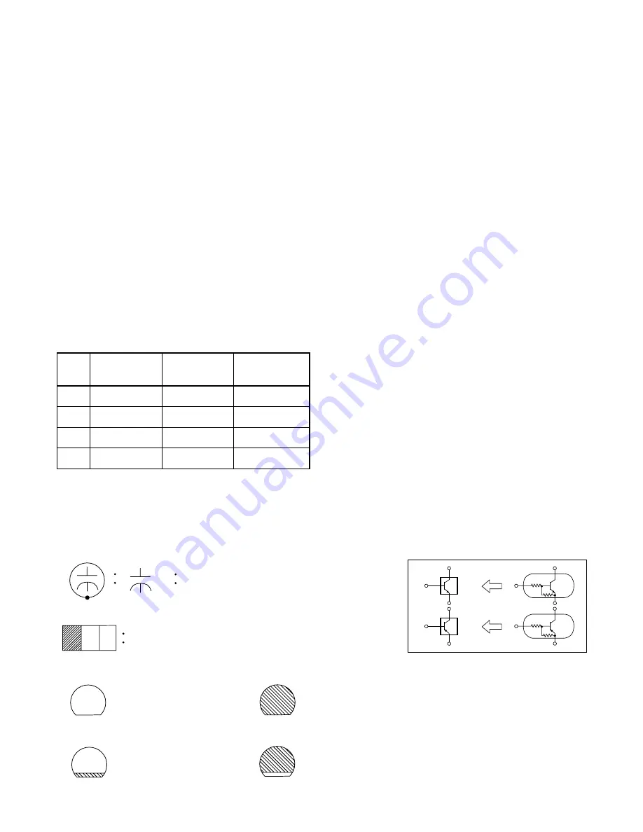
Transistor or Digital Transistor
NPN Transistor
PNP Transistor
NPN Digital Transistor
PNP Digital
Transistor
(Top View)
(Top View)
E C B
E C B
Digital Transistor
CBA Symbols
Schematic Diagram Symbols
E C B
(Top View)
(Top View)
E C B
E C B
SCHEMATIC DIAGRAMS / CBA’S AND TEST POINTS
Standard Notes
WARNING
Many electrical and mechanical parts in this chassis
have special characteristics. These characteristics
often pass unnoticed and the protection afforded by
them cannot necessarily be obtained by using replace-
ment components rated for higher voltage, wattage,
etc. Replacement parts that have these special safety
characteristics are identified in this manual and its
supplements; electrical components having such fea-
tures are identified by the mark "
!
" in the schematic
diagram and the parts list. Before replacing any of
these components, read the parts list in this manual
carefully. The use of substitute replacement parts that
do not have the same safety characteristics as speci-
fied in the parts list may create shock, fire, or other
hazards.
Capacitor Temperature Markings
Notes:
1. Do not use the part number shown on these draw-
ings for ordering. The correct part number is shown
in the parts list, and may be slightly different or
amended since these drawings were prepared.
2. All resistance values are indicated in ohms
(K=10
3
, M=10
6
).
3. Resistor wattages are 1/4W or 1/6W unless other-
wise specified.
4. All capacitance values are indicated in
µ
F
(P=10
-6
µ
F).
5. All voltages are DC voltages unless otherwise
specified.
6. Electrical parts such as capacitors, connectors,
diodes, IC’s, transistors, resistors, switches, and
fuses are identified by four digits. The first two dig-
its are not shown for each component. In each
block of the diagram, there is a note such as shown
below to indicate these abbreviated two digits.
Capacitors and transistors are represented by the following symbols.
Mark
Capacity
change rate
Standard
temperature
Temperature
range
(B)
±
10%
20°C
-25~+85°C
(F)
+30 - 80%
20°C
-25~+85°C
(SR)
±
15%
20°C
-25~+85°C
(Z)
+30 - 80%
20°C
-10~+70°C
Summary of Contents for VCR425
Page 22: ...1 8 6 1 8 7 1 8 8 HC341SCM2 Main 2 4 Schematic Diagram...
Page 23: ...1 8 9 1 8 10 1 8 11 HC341SCM3 Main 3 4 Schematic Diagram...
Page 25: ...Jack Schematic Diagram 1 8 15 1 8 16 HC341SCJ...
Page 26: ...1 8 17 1 8 18 Function Schematic Diagram HC341SCF...
Page 29: ...Jack CBA Top View Jack CBA Bottom View BHC400F01018 E 1 8 25 1 8 26...
Page 30: ...Function CBA Top View Function CBA Bottom View 1 8 27 1 8 28 BHC400F01018 B...
Page 49: ...2 4 6 U25PALDA S 12 19 Cap Belt Fig DM11 Fig DM12 20 C 1 21...
Page 55: ...3 1 1 HC341FEX A1X EXPLODED VIEWS Front Panel...
Page 74: ...VCR425 HC341ED...


