background image

LTC4260

15

4260fc

For more information 

www.linear.com/LTC4260

applicaTions inForMaTion

Power Bad Present/Power Bad Fault
When  the  FB  pin  drops  below  its 3.41V  threshold  the 

power bad present bit, C3, goes high. This pulls the GPIO 

pin low immediately when configured as PWRGD. If the 

FB pin subsequently rises back above the threshold, the 

GPIO pin will return to a high impedance state and bit C3 

will be cleared.
The power bad fault bit, D3, is set when the GATE-to-

SOURCE voltage is high and the power bad present C3 

bit is high. This blanking with the gate voltage prevents 

false power bad faults during power-up or power-down.

Fault Alerts
When any of the fault bits in FAULT register D are set, 

an optional I

2

C bus alert can be generated by setting the 

appropriate bit in the ALERT register B. This allows only 

selected faults to generate alerts. At power-up the default 

state is to not alert on faults. If an alert is enabled, the cor-

responding fault will cause the 

ALERT

 pin to pull low. After 

the bus master controller broadcasts the Alert Response 

Address, the LTC4260 responds with its address on the 

SDA line and releases 

ALERT

 as shown in Figure 11. If 

there is a collision between two LTC4260s responding 

with their addresses simultaneously, then the device with 

the lower address wins arbitration and responds first. The 

ALERT

 line will also be released if the device is addressed 

by the bus master.

+

1.235V

GND

MOTHERBOARD

CONNECTOR

PLUG-IN

CARD

SOURCE

OUT

LTC4260

10µA

23

6

BD_PRST 14

C

BD_PRST

LOAD

4260 F04

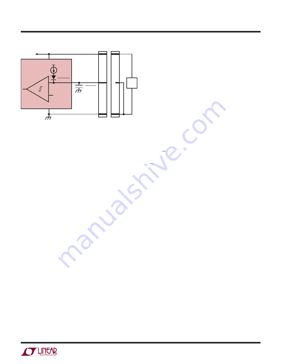
Figure 4. Plug-In Card Insertion/Removal

Once the 

ALERT

 signal has been released for one fault, 

it will not be pulled low again until the FAULT register 

indicates  a  different  fault  has  occurred  or  the  original 

fault is cleared and it occurs again. Note that this means 

repeated or continuing faults will not generate alerts until 

the associated FAULT register bit has been cleared. 

Resetting Faults
Faults are reset with any of the following conditions. First, 

a serial bus command writing zeros to the FAULT register 

D will clear the associated faults. Second, the entire FAULT 

register is cleared when the switch is turned off by either 

the ON pin or bit A3 going from high to low, or if the UV 

pin is brought below its 1.23V reset threshold, or if INTV

CC


falls below its 3.8V undervoltage lockout threshold. Finally, 

when 

BDPRST

 is brought from high to low, only FAULT 

bits D0-D3 and D5 are cleared, the bit D4 that indicates a 

BDPRST

 change of state will be set. Faults that are still 

present (as indicated in the STATUS Register C) cannot 

be cleared. 
The FAULT register will not be cleared when autoretrying. 

When autoretry is disabled the existence of a D0, D1 or D2 

fault keeps the switch off. As soon as the fault is cleared, 

the switch will turn on. If autoretry is enabled, then a high 

value in C0, C1 or C2 will hold the switch off and the FAULT 

register is ignored. Subsequently, when the C0, C1 and 

C2 bits are cleared, the switch is allowed to turn on again.

Data Converter
The LTC4260 incorporates an 8-bit data converter that 

continuously monitors three different voltages. The Δ∑ 

architecture inherently averages signal noise during the 

measurement period. The SOURCE pin uses a 1/40 resis-

tive divider to monitor a full-scale voltage of 102.4V with 

0.4V resolution (divider converts 102.4V to 2.56V). The 

ADIN pin is monitored with a 2.56V full scale and 10mV 

resolution, and the voltage between the V

DD

 and SENSE 

pins is monitored with a 76.8mV full scale and 300µV 

resolution.
The results from each conversion are stored in registers 

E, F and G and are updated 10 times per second. Setting 

CONTROL register bit A5 invokes a test mode that halts 

the data converter updates  so that registers E, F and G 

can be written to and read from for software testing. 

Summary of Contents for LTC4260

Page 1: ...o Live Backplane n 8 Bit ADC Monitors Current and Voltage n I2C SMBus Interface n Wide Operating Voltage Range 8 5V to 80V n High Side Drive for External N Channel MOSFET n Input Overvoltage Undervolt...

Page 2: ...age Temperature Range GN SW Packages 65 C to 150 C UH Package 65 C to 125 C Lead Temperature Soldering 10 sec GN SW Packages Only 300 C Supply Voltages VDD 0 3V to 100V Input Voltages SENSE VDD 10V or...

Page 3: ...resis l 70 90 120 mV IOV IN OV Pin Input Current VOV 3 5V l 0 1 A VUV TH UV Pin Threshold Voltage VUV Rising l 3 43 3 5 3 56 V VUV HYST UV Pin Hysteresis l 310 380 440 mV IUV IN UV Pin Input Current V...

Page 4: ...0 5 3 s tPHL SENSE VDD SENSE High to GATE Low VDD SENSE 200mV CGATE 10nF l 0 4 1 s ADC Resolution No Missing Codes Note 4 l 8 Bits Integral Nonlinearity VDD SENSE Note 5 SOURCE ADIN l l l 0 5 0 5 0 5...

Page 5: ...Maximum Ratings may cause permanent damage to the device Exposure to any Absolute Maximum Rating condition for extended periods may affect device reliability and lifetime Note 2 All currents into devi...

Page 6: ...75 100 TEMPERATURE C 50 0 34 UV HYSTERESIS V 0 35 0 36 0 37 0 38 0 39 25 0 25 50 4260 G03 75 100 TEMPERATURE C 50 1 220 ON BD_PRST LOW HIGH THRESHOLD V 1 225 1 230 1 235 1 240 1 245 25 0 25 50 4260 G0...

Page 7: ...75 100 IGATE A 0 GATE DRIVE V GATE V SOURCE V 8 10 12 20 4260 G10 6 4 0 5 10 15 2 16 14 VDD 80V VDD 48V VDD 12V VDD V 5 GATE DRIVE V GATE V SOURCE V 12 14 16 20 30 4260 G11 10 8 10 15 25 35 85 C 25 C...

Page 8: ...turn on rate and compensates the active current limit During turn off there is a 1mA pull down current During a short circuit or undervoltage lockout VDD or INTVCC a 600mA pull down current source be...

Page 9: ...n also serves as the ADC input to monitor output voltage The pin provides a return for the gate pull down circuit and as a supply for the charge pump circuit TIMER TimerInput Connectacapacitorbetweent...

Page 10: ...V 2V PWRGD FET ON PG RST BP BOARD PRESENT 1 235V 0 2V LOGIC TM2 UVLO2 ON UVLO1 FB OV GN UH ONLY BD_PRST ON 10 A SDAI SDAO SCL ALERT ADR0 ADR1 ADR2 GND UH ONLY EXPOSED PAD VDD ADIN 1 OF 27 8 3 8V VCC U...

Page 11: ...erheating At this point the TIMER pin ramps down us ing the 2 A current source until the voltage drops below tSU DAT tSU STO tSU STA tBUF tHD STA tSP tSP tHD DATO tHD DATI tHD STA START CONDITION STOP...

Page 12: ...ol registers are set or cleared as described in the register section After the power on reset pulse the LTC4260 will go through the following turn on sequence First the UV and OV pins must indicate th...

Page 13: ...nst excessive power dissipation in theswitchduringactivecurrentlimit theavailablecurrent is reduced as a function of the output voltage sensed by the FB pin The device also features a variable overcur...

Page 14: ...f UV is below its 3 12VthresholdafterINTVCCcrossesits4 5Vundervoltage lockout threshold an undervoltage fault will be logged in the fault register Board Present Change of State Whenever the BD PRST pi...

Page 15: ...s means repeated or continuing faults will not generate alerts until the associated FAULT register bit has been cleared Resetting Faults Faults are reset with any of the following conditions First a s...

Page 16: ...H there is a chance that the supply could collapse before the active current limit circuit brings down the GATE pin In this case the undervoltage monitors turn off the pass FET The undervoltage lockou...

Page 17: ...R2 R3 R7 and R8 for the UV OV and PG threshold voltages VOVRISING 71 2V VOVFALLING 69 44V using VOV TH 3 5V rising and 3 41V falling VUVRISING 43V VUVFALLING 38 5V using VUV TH 3 5V rising and 3 12V...

Page 18: ...e SMBus Alert Response Protocol Applications Information Acknowledge The acknowledge signal is used for handshaking between thetransmitterandthereceivertoindicatethatthelastbyte of data was received T...

Page 19: ...begins by sending a START bit followed by the special Alert Response Address 0001 100 b with the R W bit set to one Any LTC4260 that is pulling its ALERT pin low will acknowledge and begin sending ba...

Page 20: ...SLAVE TO MASTER A ACKNOWLEDGE LOW A NOT ACKNOWLEDGE HIGH R READ BIT HIGH W WRITE BIT LOW S START CONDITION P STOP CONDITION COMMAND DATA X X X X X b2 b0 0 W 0 0 0 b7 b0 A A A P S ADDRESS 1 0 a4 a0 COM...

Page 21: ...X L L L 5 8A 1 0 0 0 1 0 1 X L H H 6 8C 1 0 0 0 1 1 0 X L L NC 7 8E 1 0 0 0 1 1 1 X L L H 8 90 1 0 0 1 0 0 0 X NC NC L 9 92 1 0 0 1 0 0 1 X NC H NC 10 94 1 0 0 1 0 1 0 X NC NC NC 11 96 1 0 0 1 0 1 1...

Page 22: ...A7 6 GPIO Configure Configures Behavior of GPIO Pin FUNCTION A6 A7 GPIO PIN Power Good Default 0 0 GPIO C3 Power Bad 0 1 GPIO C3 General Purpose Output 1 0 GPIO B6 General Purpose Input 1 1 GPIO Hi Z...

Page 23: ...tage Condition 1 Enable Alert 0 Disable Alert Default B0 Overvoltage Alert Enables Alert for Overvoltage Condition 1 Enable Alert 0 Disable Alert Default Table 5 STATUS Register C 02h Read Only BIT NA...

Page 24: ...was High and Gate was High or Low D2 Overcurrent Fault Occurred Indicates Overcurrent Fault Occurred 1 Overcurrent Fault Occurred 0 No Overcurrent Faults D1 Undervoltage Fault Occurred Indicates Input...

Page 25: ...I SCL ALERT ON Figure 12 12A 12V Card Resident Application Figure 13 3A 48V Card Resident Application 16 6 17 UV BACKPLANE PLUG IN CARD R3 2 67k 1 R2 1 74k 1 4 5 9 10 8 7 2 1 24 23 18 13 20 14 12 19 1...

Page 26: ...0 25 0532 0688 1 35 1 75 008 012 0 203 0 305 TYP 004 0098 0 102 0 249 0250 0 635 BSC 033 0 838 REF 254 MIN RECOMMENDED SOLDER PAD LAYOUT 150 165 0250 BSC 0165 0015 045 005 DIMENSION DOES NOT INCLUDE M...

Page 27: ...004 012 0 102 0 305 093 104 2 362 2 642 050 1 270 BSC 014 019 0 356 0 482 TYP 0 8 TYP NOTE 3 009 013 0 229 0 330 016 050 0 406 1 270 291 299 7 391 7 595 NOTE 4 45 010 029 0 254 0 737 420 MIN 325 005...

Page 28: ...LL NOT EXCEED 0 20mm ON ANY SIDE 5 EXPOSED PAD SHALL BE SOLDER PLATED 6 SHADED AREA IS ONLY A REFERENCE FOR PIN 1 LOCATION ON THE TOP AND BOTTOM OF PACKAGE PIN 1 TOP MARK NOTE 6 0 40 0 10 31 1 2 32 BO...

Page 29: ...TE DESCRIPTION PAGE NUMBER B 1 12 Revised Conditions and Min value for IGATE FST Corrected typographical error in Layout Considerations section 3 17 C 5 13 Removed erroneous temperature dot from VGPIO...

Page 30: ...TC4252 48V Hot Swap Controller in MSOP Fast Active Current Limiting with Drain Accelerated Response Supplies from 15V LT4256 Positive 48V Hot Swap Controller with Open Circuit Detect Foldback Current...

Reviews: