background image

5

dc2518af

DEMO MANUAL DC2518A

QUICK START PROCEDURE

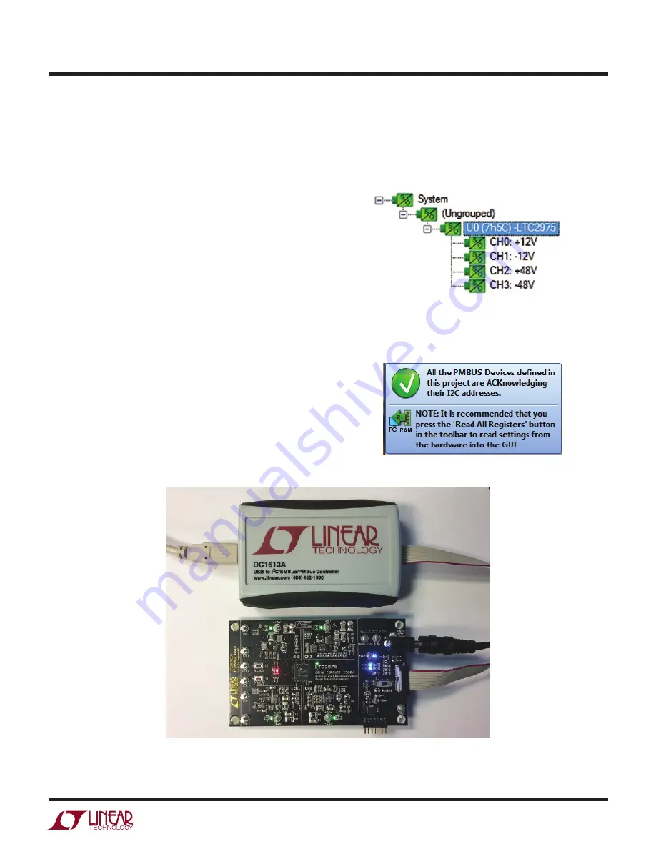
The following procedure describes how to set up a DC2518A 

demo system.
1. Download and install the LTpowerPlay GUI:
  

www.linear.com/ltpowerplay

2. Remove the board from the ESD protective bag and 

place it on a level surface. Connect the DC1613 I

2

C/

SMBus/PMBus controller to the DC2518A board using 

the 12-pin ribbon cable.

3. Confirm that the RUN switch is set to its OFF position.
4.  Plug the DC1613 USB-to-I

2

C/SMBus/PMBus controller 

into a USB port on your PC. The board should power up 

with the LED labeled “LTC2975 ON” illuminated green. 

5. Connect a +12VDC power supply with > 1A capacity to 

the V

IN

 input jack of the DC2518A board. The blue LEDs 

will illuminate indicating that DC jack power and input 

power to the LDOs is applied. Move the RUN switch to 

the ON position. The four outputs will power up and 

the green LEDs will illuminate. 

6. Launch the LTpowerPlay GUI. 

a. The GUI automatically identifies the DC2518A and 

builds a system tree for each I

2

C device. The system 

tree on the left hand side will look like this: 

Figure 3. Connecting DC2518A and the DC1613 USB to I

2

C/SMBus/PMBus Controller

b. A green message box will be displayed momentarily 

in the lower left hand corner confirming that the 

DC2518A is communicating.

Summary of Contents for DC2518A

Page 1: ...of the LTC2975 Together the LTpowerPlay software and DC2518A hardware system create a power ful development environment for designing and testing configurationsettingsoftheLTC2975 LTpowerPlaystores th...

Page 2: ...Voltage Range Programmable VSENSEP n 0V to 6V Low Resolution 0V to 3 8V High Resolution Voltage Supervisor Sensing Resolution 0V to 3 8V Range 4 096 1024 0V to 6V Range 8 192 1024 4mV LSB 8mV LSB Volt...

Page 3: ...r devices in a power system Rail ThefinaloutputvoltagethattheLTC2975supervises Supervise The act of quickly responding to a voltage andcurrentconditionthatiscomparedtopre programmed values Trim Theact...

Page 4: ...scheme in a system or to diagnose power LTpowerPlay GUI SOFTWARE issues when bringing up rails LTpowerPlay utilizes the DC1613I2C SMBus PMBusControllertocommunicatewith oneofmanypotentialtargets inclu...

Page 5: ...the LED labeled LTC2975 ON illuminated green 5 Connect a 12VDC power supply with 1A capacity to the VIN input jack of the DC2518A board The blue LEDs will illuminate indicating that DC jack power and...

Page 6: ...eGUImenupull downitemDEMO DC2518A_Defaults This writes the board defaults into the LTC2975 s RAM and automatically to NVM as well 7 The LTC2975 is configured to use the RUN switch to sequence on off t...

Page 7: ...18A DC2518A DETAILS DC1613 CONNECTOR RUN SWITCH CH2 AND CH3 OUTPUTS CASCADING CONNECTOR LTC2975 PSM CH0 AND CH1 OUTPUTS PUSHBUTTON TO FORCE A RESET AND A FAULT I2 C PORTS CASCADING CONNECTOR DC JACK 1...

Page 8: ...OPERATIONS Reset the LTC2975 ToresettheLTC2975andreloadtheEEPROMcontentsinto operating memory RAM press the pushbutton switch SW2 labeled RESET Preload the Outputs Each of the outputs has preload resi...

Page 9: ...8A not only monitors each of the four outputs but can margin the outputs either high or low Margining is the operation that moves a rail up or down for testing purposes It al lows a system to be fully...

Page 10: ...y also hold the FAULT pushbutton indefinitely to demonstrate the fault behavior and retry timing COMMON BOARD OPERATIONS Clearing a Fault To clear a fault you can click the CF icon in the GUI or simpl...

Page 11: ...ext sensitiveicon IfmultipleDC2518Aboardsareconnected be sure that the desired device is selected in the system tree Notice that the EEPROM log is locked The log will not change until it is cleared by...

Page 12: ...You can think of the Respond switches as shut this channel down when another channel faults and the Propagate switches as drive the fault pin to broadcast to other channels that this channel faulted F...

Page 13: ...nvenience TheDC2518Ademoboardhastwopowersuppliesthatare capable of relatively high voltages 48V Be careful when handling the board with these channels enabled since the voltage difference between the...

Page 14: ...sistor tolerance This is the reason 0 1 resistors are used A secondary source of error comes from the ISENSEP pin current that is pulled from the divider into the LTC2975 The divider s IR drop is due...

Page 15: ...g schemes IMON current sense ampli fier and op amp with voltage translating transistor Each of the channels allows the user to try different sensing methods Zero ohm jumpers select between one or the...

Page 16: ...s connected directly to the midpoint of the two SET resistors The RSET1 and RSET2 resistor valuesarechosensuchthatthemidpointisapproximately 1 25V avoltagethatishalfoftheDAC smaximumoutput After the D...

Page 17: ...An external NFET is connected to the SET pin that when activated pulls the SET pin to GND thereby bringing VOUT to GND When the channel is disabled the VOUT_EN pin is low thereby turning the PFET on...

Page 18: ...of the boards as shown in Figure 22 Only one 12V power source is allowed SETUP PROCEDURE FOR MULTI BOARD ARRAYS 4 The USB to I2C SMBus PMBus Controller may be plugged into any board If no demo boards...

Page 19: ...to set the slave address of an I O expander which allows the addition of multiple boards to a setup The I O Figure 23 DIP Switch Set to All 0 s Figure 24 DIP Switch Set to All 1 s expander has a base...

Page 20: ...t Position Shown in Grey in the Figure Above REFERENCE DESIGNATOR SIGNAL NAME USAGE DEFAULT JP3 Bottom A0 A1 A2 DIP Switch Used to Set the Address Offset OPEN S1 CTRL Switch Used to Enable Disable Cha...

Page 21: ...21 dc2518af DEMO MANUAL DC2518A DC2518A DETAILS BOTTOM...

Page 22: ...C6101 1k 2k Array LT3090MSE GND 50m 50m 1 0k 100 2 0k GND 15V 0 1uF 0 1uF 10uF 10uF 25V GND GND 0R 0R 15V 15V 10k 140k 1k 200k 69 8k 3V3 LT6105MS8 GND 100 100 1 0k 0R 0R 130k 40 2k 3V3 GND 2N3906 3V3...

Page 23: ...0 4 7uF 25V 2 2uF 100V 1uF 100V 47nF 1nF 464k 14k 47pF GND GND 46 4k 10k 3V3 GND 16 2k 953k 0 LT8330 2 2uF 100V GND 2 2uF 100V GND 133k 33 2k 3V3 2 0k 100 100 3V3 13 7k 3 01k 13 7k GND 9 76k MMST3906...

Page 24: ...M9 R69 LED4 LED6 R71 LED5 R70 1 2 3 4 5 6 U10 C45 LED10 R94 FAULTB FAULTB RESETB SCL SDA SHARE_CLK RUN_CH0 RUN_CH1 RUN_CH2 RUN_CH3 CTRL REFP VSNSP_CH0 VSNSP_CH1 VSNSP_CH3 VDAC_CH1 VDAC_CH3 VSNSP_CH2 V...

Page 25: ...uF GND 3V3 B140 13 F B140 13 F 10m 5V 12V 30k BLUE GND 30k 30k BLUE BLUE 6 8uH 10uH GND GND 5 6 7 8 1 2 3 4 JP3 1 2 3 4 5 6 7 8 9 10 11 12 J2 2 3 1 5 6 4 S1 1 2 3 4 5 U13 C47 R75 R76 1 2 3 4 5 6 7 8 9...

Page 26: ...ORY INCLUDING ANY WARRANTY OF MERCHANTABILITY OR FITNESS FOR ANY PARTICULAR PURPOSE EXCEPT TO THE EXTENT OF THIS INDEMNITY NEITHER PARTY SHALL BE LIABLE TO THE OTHER FOR ANY INDIRECT SPECIAL INCIDENTA...

Reviews: