background image

2

dc1755af

DEMO MANUAL DC1755A

QUICK START PROCEDURE

Demonstration circuit 1755A is easy to set up to evalu-
ate the performance of the LTC3860EUH. Please refer to 
Figure 1 for proper measurement equipment setup and 
follow the procedure below.  

1) With power off, connect the input supply, load and 
  meters as shown in Figure 1. Preset the load to 0A and
  V

IN

 supply to be 0V. Place jumpers in the following 

 positions:

JP1 RUNA 

ON

JP2 RUNB 

ON

JP3 

INT PWR BLK BIAS 

ON

2) Adjust the input voltage to be between 6V to 14V. V

OUTA


  should 1.5V ± 2%.

  V

OUTB

 should 1.2V ± 2%.

3) Next, apply 50A load to each output and remeasure 
  V

OUT

.

4) Once the DC regulation is confirmed, observe the output 
  voltage ripple, load step response, efficiency and other 
 parameters.

Note 1. No airflow is required at room temperature with 
50A on both outputs. But for ambient temperatures higher 
than 30°C, a cooling fan is recommended.

Note 2. Use the BNC connectors labeled V

OUTA

 or V

OUTB


to measure the output voltage ripple.

Note 3. Do not apply the load from the VOSA

+

 turret to 

the VOSA

 turret or from the VOSB

+

 turret to the VOSB


turret. These turrets are only intended to monitor the 
voltage across COUT3 and COUT13 respectively. Heavy 
load currents applied across these turrets may damage 
the converter.

DYNAMIC LOAD CIRCUIT (OPTIONAL)

Demonstration circuit 1755A provides a simple load step 
circuit consisting of a MOSFET and sense resistor for each 
rail. To apply a load step, follow the steps below.

1) Preset the amplitude of a pulse generator to 0.0V and 
  the duty cycle to 5% or less.

2) Connect the scope to the VOUT BNC connectors for 
  the rail under test with a coax cable. To monitor the 
  load step current, connect the scope probe across the 
 ISTEP

+–

 turrets for that rail.

3) Connect the output of the pulse generator to the PULSE 
  GEN turret for the rail under test and connect the return 
  to one of the GND turrets.

4) With the converter running, slowly increase the 
  amplitude of the pulse generator output to provide the 
  desired load step pulse height. The scaling for the load 
  step signal is 10mV/A.

Summary of Contents for DC1755A

Page 1: ...logy Corporation All other trademarks are the property of their respective owners PERFORMANCE SUMMARY The main features of the board are listed below High efficiency and high current density Remote sensing for each output Optional resistors to tie the two outputs together Connectorandheadertotietwoormoreboardstogether for up to 12 phase operation RUN PGOOD and TRACK SS pins for each output CLKIN a...

Page 2: ...TA or VOUTB to measure the output voltage ripple Note 3 Do not apply the load from the VOSA turret to the VOSA turret or from the VOSB turret to the VOSB turret These turrets are only intended to monitor the voltage across COUT3 and COUT13 respectively Heavy load currents applied across these turrets may damage the converter DYNAMIC LOAD CIRCUIT OPTIONAL Demonstration circuit 1755A provides a simp...

Page 3: ... Figure 1 Proper Measurement Equipment Setup IOUTA A A IIN VIN supply V VOUTA V VOUTA load VOUTB load A IOUTB V VOUTB VIN Monitor voltage across COUT7 and COUT19 for accurate efficiency measurements DC1755a F01 QUICK START PROCEDURE ...

Page 4: ...errighthandcorner Totie thetwooutputstogether makethefollowingmodifications 1 Select one rail to be the master a If VOUTA is the master then stuff 0Ω at R103 to disable the error amplifier for VOUTB b If VOUTB is the master then stuff 0Ω at R104 to disable the error amplifier for VOUTA 2 Stuff 0Ω at R87 R88 R89 and R91 to tie the IAVG COMP TRACK SS and RUN signals together 3 Remove the redundant c...

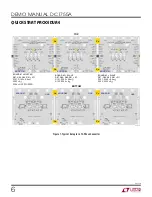
Page 5: ...the slave Figure 6 shows the typical setup for a 6 phase 2 phase converter Figure 7 shows the typical setup for a 12 phase converter For additional help and support contact your local LTC sales office BOARD 2 SIDE A SLAVE SIDE B INDEPENDENT DUAL PHASE RAIL R87 R88 R89 R91 NOT STUFFED R101 R102 NOT STUFFED R103 NOT STUFFED R104 0 Cu GND GND TOP BOTTOM BOARD 1 BOARD 2 BOARD 2 BOARD 1 BOARD 1 MASTER ...

Page 6: ...BOTTOM BOARD 1 BOARD 2 BOARD 3 BOARD 3 BOARD 2 BOARD 1 BOARD 1 MASTER R87 R88 R89 R91 0 R101 R102 0 0m R103 0 R104 NOT STUFFED BOARD 2 SLAVE R87 R88 R89 R91 0 R101 R102 0 0m R103 R104 0 BOARD 3 SLAVE R87 R88 R89 R91 0 R101 R102 0 0m R103 R104 0 Cu Cu Cu Cu Cu Cu Cu DC1755a F07 QUICK START PROCEDURE ...

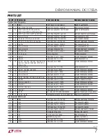
Page 7: ...18 RES 0603 0Ω JUMPER VISHAY CRCW06030000Z0EA 16 2 R1 to A R1 to B RES 0603 20k 1 1 10W NIC NRC06F2002TRF 17 6 R2 R17 R37 R51 R57 R107 RES 0603 1Ω 5 1 10W VISHAY CRCW06031R00JNEA 18 2 R2 to A R2 to B RES 0603 6 8k 1 1 10W VISHAY CRCW06036K80FKEA 19 2 R3 to A R3 to B RES 0603 523Ω 1 1 10W VISHAY CRCW0603523RFKEA 20 9 R3 R4 R24 R26 R31 R38 R39 R61 R63 RES 0603 10k 1 1 10W VISHAY CRCW060310K0FKEA 21 ...

Page 8: ...2 R87 R88 R89 R91 R92 R94 R95 R96 R103 R104 R108 R110 R111 R114 R115 R117 R119 RES 0603 OPTIONAL 6 0 C3 C5 C6 C12 C15 C17 C18 C24 CAP 0603 OPTIONAL 7 0 Q2 Q3 MOSFET TO 252 OPTIONAL 8 0 R73 R74 R77 R78 R83 R84 R85 R86 RES 0603 OPTIONAL 9 0 R80 R82 R101 R102 RES 2010 OPTIONAL 10 2 Q1 Q4 MOSFET TO 252 VISHAY SUD50N03 09P 11 2 R75 R76 RES 0603 10k 1 1 10W VISHAY CRCW060310K0FKEA 12 2 R79 R81 RES 2010 ...

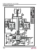
Page 9: ...E WITH LINEAR TECHNOLOGY PARTS SCALE NONE www linear com 2 Monday January 16 2012 1 3 DUAL OUTPUT 4 PHASE STEP DOWN CONVERTER AK MIKE S N A LTC3860EUH DEMO CIRCUIT 1755A R6 OPT R6 OPT U1 LTC3860EUH U1 LTC3860EUH VCC 1 FB1 2 COMP1 3 VSNSOUT 4 VSNSN 5 VSNSP 6 COMP2 7 FB2 8 TRK SS2 9 RUN2 17 ILIM2 18 PWM2 16 ISNS1N 21 ISNS2N 20 ISNS1P 22 ILIM1 23 RUN1 24 PWM1 25 IAVG 28 ISNS2P 19 FREQ 10 CLKIN 11 CLK...

Page 10: ... DOWN CONVERTER AK MIKE S N A LTC3860EUH DEMO CIRCUIT 1755A C13 0 22uF C13 0 22uF C17 OPT C17 OPT R36 0 R36 0 E27 VOSB E27 VOSB R113 0 R113 0 R54 0 R54 0 R61 10K R61 10K E10 PGOODB E10 PGOODB COUT13 330uF 2 5V COUT13 330uF 2 5V COUT18 100uF 6 3V 1206 COUT18 100uF 6 3V 1206 U2 LTC3860EUH U2 LTC3860EUH VCC 1 FB1 2 COMP1 3 VSNSOUT 4 VSNSN 5 VSNSP 6 COMP2 7 FB2 8 TRK SS2 9 RUN2 17 ILIM2 18 PWM2 16 ISN...

Page 11: ...RCUIT THAT MEETS CUSTOMER SUPPLIED SPECIFICATIONS HOWEVER IT REMAINS THE CUSTOMER S RESPONSIBILITY TO VERIFY PROPER AND RELIABLE OPERATION IN THE ACTUAL APPLICATION COMPONENT SUBSTITUTION AND PRINTED CIRCUIT BOARD LAYOUT MAY SIGNIFICANTLY AFFECT CIRCUIT PERFORMANCE OR RELIABILITY CONTACT LINEAR TECHNOLOGY APPLICATIONS ENGINEERING FOR ASSISTANCE THIS CIRCUIT IS PROPRIETARY TO LINEAR TECHNOLOGY AND ...

Page 12: ...LUDING ANY WARRANTY OF MERCHANTABILITY OR FITNESS FOR ANY PARTICULAR PURPOSE EXCEPT TO THE EXTENT OF THIS INDEMNITY NEITHER PARTY SHALL BE LIABLE TO THE OTHER FOR ANY INDIRECT SPECIAL INCIDENTAL OR CONSEQUENTIAL DAMAGES The user assumes all responsibility and liability for proper and safe handling of the goods Further the user releases LTC from all claims arising from the handling or use of the go...

Page 13: ...Mouser Electronics Authorized Distributor Click to View Pricing Inventory Delivery Lifecycle Information Analog Devices Inc DC1755A ...

Reviews: