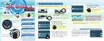
3.2.2 GSM Transmitter
The RTR6275 transmitter outputs(DA_HB2_OUT and DA_LB1_OUT)include on-chip output matching
inductors. The 50ohm output impedance is achieved by adding a series capacitor at the output pins.
The capacitor value may be optimized for specific applications and PCB characteristics based on pass-
band symmetry about the band center frequency, the suggested starting value is shown in Figure1.3.
The RTR6275 IC is able to support GSM 900 and GSM 1800/1900 mode transmitting. This design
guideline shows a tri-band GSM application.
Both high-band and low band outputs are followed by resistive pads to ensure that the load presented
to the outputs remains close to 50ohm. The low-band GSM Tx path also includes a Tx-band SAW filter
to remove noise-spurious components and noise that would be amplified by the PA and appear in the
GSM Rx band
3. TECHNICAL BRIEF
- 22 -
91
91
6pF
100
100
51
12pF
39
Ω
Ω
Ω
Ω
Ω
Ω
[Fig 1.3] GSM Transmitter matching
Summary of Contents for U250
Page 1: ...Date June 2007 Issue 1 0 Service Manual Model U250 KU250 Service Manual U250 KU250 ...
Page 3: ... 4 ...
Page 20: ...3 TECHNICAL BRIEF 21 Fig 1 2 RTR6275 RX feature ...
Page 28: ...3 TECHNICAL BRIEF 29 Figure1 7 PM6650 Block Diagram ...
Page 41: ...3 TECHNICAL BRIEF 42 Table 1 2 Description of RF configurations ...
Page 45: ...3 TECHNICAL BRIEF 46 Figure 1 12 PM6650 Functional Block Diagram ...
Page 72: ...4 TROUBLE SHOOTING 73 4 1 RF Component 4 TROUBLE SHOOTING LGMC ...
Page 73: ...4 TROUBLE SHOOTING 74 Block Diagram Block Ref Name UMTS Part Name Function Comment ...
Page 77: ...4 TROUBLE SHOOTING 78 Check C312 of PMIC U300 Check R213 of MSM U201 T ...
Page 81: ...4 TROUBLE SHOOTING 82 ...
Page 84: ...4 TROUBLE SHOOTING 85 ...
Page 85: ...4 TROUBLE SHOOTING 86 4 7 Checking GSM Block 1 3 2 ...
Page 87: ...4 7 3 Checking RF Tx level 4 TROUBLE SHOOTING 88 ...
Page 90: ...4 TROUBLE SHOOTING 91 ...
Page 97: ...4 TROUBLE SHOOTING 98 R313 Q301 Q302 Q300 Charging part Main PCB Front ...
Page 107: ...4 TROUBLE SHOOTING 108 R422 R421 U401 ...
Page 109: ...4 TROUBLE SHOOTING 110 C401 C402 R406 C407 CN401 ...
Page 111: ...4 TROUBLE SHOOTING 112 Analog Switch Audio Amp SPK ...
Page 113: ...4 TROUBLE SHOOTING 114 MIC400 C417 R424 ...
Page 115: ...4 TROUBLE SHOOTING 116 Ear_Sense_N MIC Input ...
Page 117: ...4 TROUBLE SHOOTING 118 VPWR MOTOR_PWR ...
Page 134: ...6 BLOCK DIAGRAM 135 Table 2 1 RF Block Component ...
Page 136: ...6 BLOCK DIAGRAM 137 6 2 2 Memory Interface Fig 2 3 Memory Interface Diagram ADDRESS 14 0 ...
Page 137: ...6 BLOCK DIAGRAM 138 6 2 3 USB UART SIM JTAG Interface Fig 2 4 USB UART SIM JTAG Interface ...
Page 139: ...6 BLOCK DIAGRAM 140 6 2 4 Placement Top Side LGMC ...
Page 140: ...6 BLOCK DIAGRAM 141 Bottom Side LGMC ...
Page 141: ... 142 ...
Page 146: ... 147 LGMC 8 PCB LAYOUT U250 KU250 ...
Page 147: ... 148 LGMC 8 PCB LAYOUT U250 KU250 ...
Page 157: ... 158 ...
Page 174: ...Note ...
Page 175: ...Note ...