background image

3-6

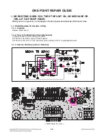
ONE POINT REPAIR GUIDE

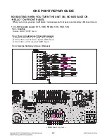
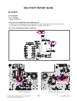
NO BOOTING WHEN YOU TURN THE UNIT ON, NO MESSAGE OR 
“HELLO” ON FRONT PANEL

When you turn on your set, it will blank / no message on front panel, and stand-by LED doesn’t work.

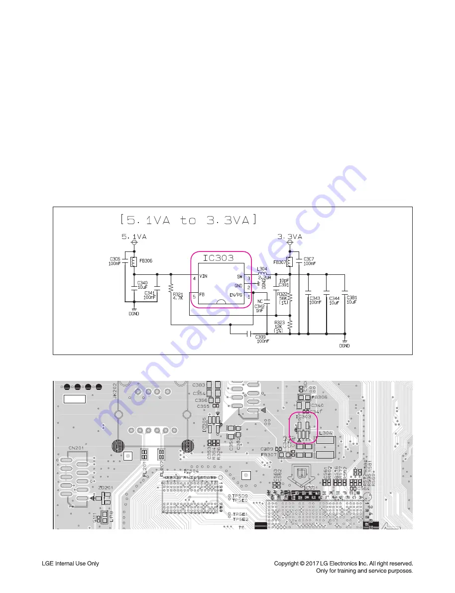
1-2. IC303 System 3.3 V (No 3.3 VA)

1-2-1. Solution

Replace MAIN/ FRONT board.

1-2-2. How to troubleshoot (Countermeasure)

1) Please check 3.3 VA of IC303 pin3.
2) If 3.3 VA is abnormal, replace MAIN board.
3) If 5.1 VA is OK, replace FRONT board.

1-2-3. Service hint (Any picture / Remark)

< MAIN board top view >

IC303

IC303

L304

L304

Summary of Contents for SJ9

Page 1: ...s STRICTLY PROHIBITED unless you have obtained the prior written consent of the LG Electronics entity from which you received this Service Manual The material covered by this prohibition includes without limitation any text graphics or logos in this Service Manual Copyright 2017 LG Electronics Inc All right reserved Only for training and service purposes CONFIDENTIAL SMARTHi FiAUDIO WirelessMulti ...

Page 2: ...Copyright 2018 LG Electronics Inc All rights reserved Only for training and service purposes CONTENTS SECTION 1 SUMMARY SECTION 2 CABINET MAIN CHASSIS SECTION 3 ELECTRICAL SECTION 4 WIRELESS SUBWOOFER PART ...

Page 3: ...ONTENTS PRODUCT SAFETY SERVICING GUIDELINES FOR AUDIO PRODUCTS 1 3 SERVICING PRECAUTIONS 1 4 GENERAL SERVICING PRECAUTIONS INSULATION CHECKING PRODEDURE ELECTROSTATICALLY SENSITIVE ES DEVICES NAME OF EACH COMPONENT 1 5 WIRELESS SUBWOOFER CONNECTION 1 6 HIDDEN KEY MODE 1 7 SOFTWARE UPDATE GUIDE 1 8 SPECIFICATIONS 1 16 ...

Page 4: ...ign Be sure that the safety purpose of the polarized line plug has not been defeated 3 Soldering must be inspected to discover possible cold solder joints solder splashes or sharp solder points Be certain to remove all loose foreign particles 4 Check for physical evidence of damage or deterioration to parts and components for frayed leads or damaged insulation including the AC cord and replace if ...

Page 5: ... more than 1Mohm Note 1 Accessible Conductive Parts include Metal panels Input terminals Earphone jacks etc Electrostatically Sensitive ES Devices Some semiconductor solid state devices can be damaged easily by static electricity Such components commonly are called Electrostatically Sensitive ES Devices Examples of typical ES devices are integrated circuits and some field effect transistors and se...

Page 6: ... Volume Wi Fi Ntssjhyx nsnynfq Xzxnh Qqt uwtizhy yt tzw sjy twp nwjqjxxq Add Liix ymj fiinyntsfq Xzxnh Qqt uwtizhy yt tzw sjy twp Ts hfxj ymfy tsj tw rtwj Xzxnh Qqt uwtizhy nx htssjhyji B USB Service only b it sqtfi htssjhytw C LAN port D PORTABLE IN connector E OPTICAL IN connector F HDMI OUT TV ARC Ntssjhy yt SOXT TY L N ts _a G HDMI IN Rear panel NAME OF EACH COMPONENT Front Panel Rear Panel so...

Page 7: ...reless subwoofer does not make sound To solve the problem follow the steps below 1 Press Pairing button on the rear of the wireless subwoofer The green LED on the front of the wireless subwoofer blinks quickly 2 Turn on the sound bar 3 Pairing is completed The green LED on the front of the wireless subwoofer turns on Note It takes a few seconds and may take longer for the main unit and the subwoof...

Page 8: ...Remote control SOUND EFFECT for more than 3 seconds VERSION CHECK Main unit Volume Remote control Play Pause for more than 3 seconds Next Forward Skip Previous Backward Skip Exit Power off Woofer TX Reset Main unit MIN volume minimum state Remote control Mute for about 5 seconds Woofer RX Reset RESET on the woofer for 3 seconds HIDDEN KEY MODE ...

Page 9: ...HDMI_SJ9 BIN if USB driver is E WIRELESS TX E WIRELESS_TX bin if USB driver is E WIRELESS RX E WIRELESS_RX bin if USB driver is E 1 2 Update 1 Power on 2 Insert USB When connecting USB to the main unit you can connect easily using USB Gender 3 When display UPDATE on LCD press play pause key on remote control and proceed update 4 Never remove USB or AC cord while updating 5 During the update LCD is...

Page 10: ...s Inc All rights reserved Only for training and service purposes 2 Using APP Power on Smart Audio and implement Music Flow App in your smart phone 1 Connect Speaker 3 Settings Version Info 2 Select red box 4 Select Device version info ...

Page 11: ...ectronics Inc All rights reserved Only for training and service purposes Using APP 5 Display Need to update if there are new firmware in the server 6 Start Update below icon Display new version info if you press Need to update ...

Page 12: ...right 2018 LG Electronics Inc All rights reserved Only for training and service purposes Do not power off during update 7 Display update info 8 Display Update is completed message when Complete update Using APP ...

Page 13: ...1 12 Copyright 2018 LG Electronics Inc All rights reserved Only for training and service purposes 3 Using MP tool 1 Open MP tool and select Key DN 2 Check the section for download and open download file ...

Page 14: ... Gateway 10 168 0 1 4 Set power on 5 Connect LAN cable to Set and then Press ADD key within 3 seconds after connect the LAN Please connect the LAN when blinking WiFi LED after booting Download file name B E LG_NB_C003M06 ROM MICOM MICOM_SJ9 HEX Caution Do not you update the B E program and MICOM program at the same time 6 Connect Status change OK if success connect MP tool Using MP tool ...

Page 15: ...1 14 Copyright 2018 LG Electronics Inc All rights reserved Only for training and service purposes 7 Press Update button 8 Download result display OK if start download Using MP tool ...

Page 16: ... You can identify update status by network indicator lamp White Updating blinking white LED Using MP tool 3 1 Version check 1 PC IP setting IP 192 168 0 1 Subnet 255 255 254 0 Gateway 10 168 0 1 2 Open MP tool 3 Set power on 4 Press ADD button after connect LAN cable 5 Display the version in the tool ...

Page 17: ... 19 Pin Type A HDMI connector x 1 4K Sources dependent on HDCP 2 2 are supported at 4K resolutions AMPLIFIER RMS Output Total 500 W RMS Front 43 W RMS x 2 4 Ω at 1 kHz THD 10 Center 43 W RMS 4 Ω at 1 kHz THD 10 Surround 43 W RMS x 2 4 Ω at 1 kHz THD 10 Top 43 W RMS x 2 4 Ω at 1 kHz THD 10 Subwoofer 200 W RMS 3 Ω at 80 Hz THD 10 WIRELESS SUBWOOFER Power requirements Refer to the main label on the s...

Page 18: ...nd service purposes SECTION 2 CABINET MAIN CHASSIS CONTENTS DISASSEMBLY INSTRUCTIONS 2 2 1 HOW TO DISASSEMBLE THE MAIN UNIT 2 2 2 HOW TO DISASSEMBLE THE SUBWOOFER 2 11 EXPLODED VIEWS 2 17 1 MAIN UNIT SECTION 2 17 2 WIRELESS SUBWOOFER SECTION 2 19 3 PACKING ACCESSORY SECTION 2 21 ...

Page 19: ... for training and service purposes DISASSEMBLY INSTRUCTIONS 1 1 2 Cover Bottom Assembly Figure 1 1 1 HOW TO DISASSEMBLE THE MAIN UNIT Before begin position the Main Unit upside down 1 1 Case Bottom Assembly 1 Remove the 36 screws 2 Remove the Case Bottom Assembly ...

Page 20: ...s reserved Only for training and service purposes 2 3 2 Cover SMPS 1 1 SPK cable Figure 1 2 2 Figure 1 2 1 HOW TO DISASSEMBLE THE MAIN UNIT 2 Remove the 4 screws 3 Remove the Cover SMPS 1 2 Cover SMPS 1 Disconnect the 3 SPK cables from the Main PCB ...

Page 21: ...ice purposes 2 2 3 2 Main Chassis Assembly WIRELESS KEY BT 1 1 Figure 1 3 2 Figure 1 3 1 HOW TO DISASSEMBLE THE MAIN UNIT 2 Remove the 3 screws 3 Remove the Main Chassis Assembly Main Chassis PCBA 1 3 Main Chassis Assembly 1 Disconnect the 3 cables from the Main PCB KEY BT and WIRELESS ...

Page 22: ... JACK PCB JACK PCB Sub Assembly Figure 1 3 1 Figure 1 3 2 HOW TO DISASSEMBLE THE MAIN UNIT 1 3 1 Front PCB Assembly 1 Remove the 2 screws 2 Remove the Front PCB Assembly 1 3 2 JACK PCB Assembly 1 Disconnect the cable 2 Remove the 2 screws 3 Remove the JACK PCB Sub Assembly 4 Remove the 6 screws 5 Remove the JACK PCB Assembly ...

Page 23: ...s 2 3 1 1 SMPS PCB 2 3 1 MAIN PCB Wi Fi Figure 1 3 3 Figure 1 3 4 HOW TO DISASSEMBLE THE MAIN UNIT 1 3 3 SMPS PCB Assembly 1 Disconnect the 2 cables 2 Remove the screw 3 Remove the SMPS PCB Assembly 1 3 4 MAIN PCB Assembly 1 Disconnect the cables 2 Remove the screw 3 Remove the MAIN PCB Assembly ...

Page 24: ...s Inc All rights reserved Only for training and service purposes HOW TO DISASSEMBLE THE MAIN UNIT 2 2 1 3 4 Figure 1 3 5 1 3 5 Wi Fi Module 1 Remove the screw 2 Remove the Wi Fi holder 3 Remove the Wi Fi module 4 Disconnect the cable ...

Page 25: ... HOW TO DISASSEMBLE THE MAIN UNIT WIRELESS BT Figure 1 4 1 4 BT and WIRELESS Module 1 Disconnect the FFC cable from the BT module 2 Disconnect the 2 hooks and then remove the BT module 3 Disconnect the FFC cable from the WIRELESS module 4 Disconnect the 2 hooks and then remove the WIRELESS module ...

Page 26: ...training and service purposes 2 1 KEY PCB Figure 1 5 Figure 1 6 HOW TO DISASSEMBLE THE MAIN UNIT 1 5 SPEAKER CHAMBER Assembly 1 Remove the Speaker Chamber Assembly 1 6 KEY PCB Assembly 1 Remove the 2 screws 2 Disconnect the 5 hooks and then remove the KEY PCB Assembly ...

Page 27: ...ights reserved Only for training and service purposes Right SPK cable Left SPK cable Center SPK cable Figure 1 7 HOW TO DISASSEMBLE THE MAIN UNIT 1 7 How to organize cables When assembling place the SPK network cables as shown in the figure below ...

Page 28: ...g and service purposes 1 2 2 1 Sub Woofer Board Assembly SPK cable Figure 2 1 1 Figure 2 1 2 2 HOW TO DISASSEMBLE THE SUBWOOFER 2 1 Sub Woofer Board Assembly 1 Remove the 4 Foot Rubbers 2 Remove the 8 screws 3 Pull out the Sub Woofer Board Assembly and disconnect the SPK cable ...

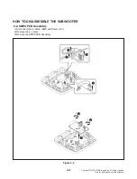
Page 29: ...l rights reserved Only for training and service purposes 1 1 1 2 2 1 3 Figure 2 2 AMP SMPS HOW TO DISASSEMBLE THE SUBWOOFER 2 2 SMPS PCB Assembly 1 Disconnect the 2 cables AMP and Power cord 2 Remove the 4 screws 3 Remove the SMPS PCB Assembly ...

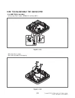
Page 30: ...erved Only for training and service purposes 1 1 KEY LED WIRELESS 3 2 2 Figure 2 3 1 Figure 2 3 2 HOW TO DISASSEMBLE THE SUBWOOFER 2 3 AMP PCB Assembly 1 Disconnect the 3 cables WIRELESS LED and KEY 2 Remove the 4 screws 3 Remove the AMP PCB Assembly AMP ...

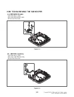
Page 31: ...d service purposes 1 3 2 2 1 3 Figure 2 4 Figure 2 5 HOW TO DISASSEMBLE THE SUBWOOFER 2 4 WIRELESS Module 1 Remove the 2 screws 2 Remove WIRELESS module 3 Disconnect the cable 2 5 LED PCB Assembly 1 Remove the 2 screws 2 Remove LED PCB Assembly 3 Disconnect the cable WIRELESS LED ...

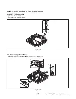
Page 32: ... Only for training and service purposes 2 1 Figure 2 6 Figure 2 7 HOW TO DISASSEMBLE THE SUBWOOFER 2 6 KEY PCB Assembly 1 Remove the 2 screws 2 Remove KEY PCB Assembly 2 7 How to organize cables When assembling place the cables as shown in the figure below KEY ...

Page 33: ...2 16 Copyright 2018 LG Electronics Inc All rights reserved Only for training and service purposes ...

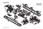
Page 34: ... 506 L K CABLE1 FRONT I 268 462 SMPS MAIN I A43 LCD01 462 506 462 462 462 462 H D J HDMI JACK A46 A47 265 A48 470 G J L B A F E C D CABLE4 462 506 506 A44A Wi Fi C 462 261 A44 A51 CABLE5 506 264 263 H 300 EXPLODED VIEWS 1 MAIN UNIT SECTION NOTES THE EXCLAMATION POINT WITHIN AN EQUILATERAL TRIANGLE IS INTENDED TO ALERT THE SERVICE PERSONNEL TO THE PRESENCE OF IMPORTANT SAFETY INFORMATION IN SERVICE...

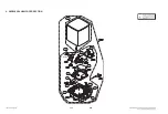
Page 35: ...392 384 393 385 387 395 388 388 395 386 WIRELESS LED AMP SMPS A81K KEY 390 A332 A330 F 389 2 WIRELESS SUBWOOFER SECTION NOTES THE EXCLAMATION POINT WITHIN AN EQUILATERAL TRIANGLE IS INTENDED TO ALERT THE SERVICE PERSONNEL TO THE PRESENCE OF IMPORTANT SAFETY INFORMATION IN SERVICE LITERATURE ...

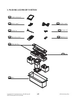
Page 36: ...2 21 804 Bag 802 Box 803 Main packing 801 Owner s manual 806 Optical cable 836 Screws 2 835 Wall bracket 808 Batteries 2 900 Remote control 829 Cable tie 3 PACKING ACCESSORY SECTION ...

Page 37: ...2 22 ...

Page 38: ...L 3 5 2 NO SOUND 3 8 3 PROTECTION ERROR 3 12 WAVEFORMS OF MAJOR CHECK POINT 3 15 1 CRYSTAL 3 15 2 FLASH 3 17 3 TACT KEY 3 17 4 REMOTE CONTROL 3 19 5 OPTICAL 3 20 CIRCUIT VOLTAGE CHART 3 21 1 ICs 3 21 2 CAPACITORS 3 22 3 CONNECTORS 3 22 PRINTED CIRCUIT BOARD DIAGRAMS 3 23 1 SMPS P C BOARD DIAGRAM 3 23 2 MAIN P C BOARD DIAGRAM 3 25 3 HDMI JACK P C BOARD DIAGRAM 3 29 4 FRONT P C BOARD DIAGRAM 3 31 5 ...

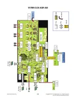
Page 39: ...mm ST SMD BT KEY 2P 1 25mm Angle SMD 2P 1 25mm ST SMD 8P 1 25mm ST SMD Wi Fi 16P 2mm Angle Header SMD MAIN PCB Wireless Rear Box 26P 0 5mm Angle SMD 26P 0 5mm Angle SMD Wireless Subwoofer 30P 2mm ST Header SMD 30P 2mm ST Socket SMD HDMI PCB HDMI HDMI Ethernet USB OPT Portable 14P 0 5mm Angle Locking SMD 14P 0 5mm Angle Locking SMD Top Bottom WIRING DIAGRAM ...

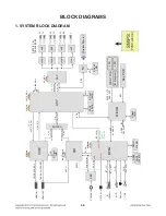
Page 40: ...3 128MB KEY SPI BL_CTL RMC LED H_D1 D3 SPDIF 2 Ch 32 MICOM UART M_RESET S Flash 1 MB SPDIF MPEG SPI0 BT_UART 24 576 MHz ARC S Flash 1MB ADC M_D0 HDMI BUFFER D0 MCLK BCK LRCK D_D0 MCLK BCK LRCK SPI H_D0 MCLK BCK LRCK BCK LRCK 24 576 MHz 24 576 MHz 27 MHz 27 MHz DAC D_D3 D D DIR DDR3 128 MB I2S 2 Ch FL TL FR TR SL SR C 40 MHz OP AMP OP AMP OP AMP OP AMP 8 Ethernet Wi Fi 12 288 MHz Multi room 48kHz R...

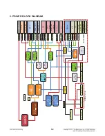
Page 41: ... 3V DAC_1 2V DAC_3 3V DAC_3 3V AMP IC 25 VA HDMI 4k HDMI_5 1VA HD_1 0V HD_3 3V ADC DIR VCC_5V D_3 3V D_3 3V OPTICAL PORTABLE HDMI IN x 1 HDMI OUT x 1 3 3 VA VCC_5V DC DC 12 VA 5 1 VA 3 3 VA 12 VA DC DC 25 VA 12 VA SW SMPS FRONT PCB JACK PCB LDO 5 1 VA DAC_3 3V LDO DAC_3 3V DAC_1 2V DC DC 5 1 VA 3 3 VA SW DSP_3 3V SW D_3 3V SW WL_3 3V DC DC 5 1 VA 3 5 V DC DC 5 1 VA D_1 5V DC DC 5 1 VA DSP_1 5V DC ...

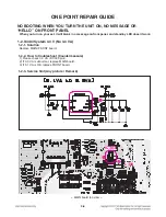
Page 42: ... by LED doesn t work 1 1 IC300 System 12 VA No 12 VA 1 1 1 Solution Replace MAIN board 1 1 2 How to troubleshoot Countermeasure 1 Please check 20 VA of IC300 pin2 VIN 2 If 20 VA is abnormal please check adapter 3 If 20 VA is OK but 12 VA is abnormal pin3 of IC300 VOUT replace MAIN board 1 1 3 Service hint Any picture Remark MAIN board top view IC300 IC300 L301 L301 ...

Page 43: ... front panel and stand by LED doesn t work 1 2 IC303 System 3 3 V No 3 3 VA 1 2 1 Solution Replace MAIN FRONT board 1 2 2 How to troubleshoot Countermeasure 1 Please check 3 3 VA of IC303 pin3 2 If 3 3 VA is abnormal replace MAIN board 3 If 5 1 VA is OK replace FRONT board 1 2 3 Service hint Any picture Remark MAIN board top view IC303 IC303 L304 L304 ...

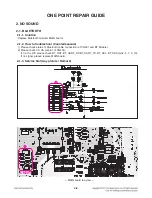
Page 44: ...anel and stand by LED doesn t work 1 3 LCD System power 12 V VCC_5V No 12 V VCC_5V 1 3 1 Solution Replace MAIN FRONT board 1 3 2 How to troubleshoot Countermeasure 1 Please check CN101 12 V pin9 VCC_5V pin4 2 If 12V VCC_5V is abnormal replace MAIN board 3 If 12V VCC_5V OK replace FRONT board 1 3 3 Service hint Any picture Remark MAIN board top view CN101 CN101 ...

Page 45: ...oot Countermeasure 1 Please check status of Bluetooth cable connection at CN201 and BT Module 2 Please check 3 3 VA at pin1 of CN201 If 3 3 V is OK please check BT_RST BT_UART_RX BT_UART_TX BT_SCL BT_SDA pin2 5 7 9 10 If no signal please replace MAIN board 2 1 3 Service hint Any picture Remark MAIN board top view CN201 CN201 ...

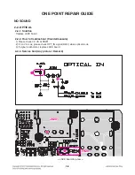
Page 46: ...ACK board 2 2 2 How to troubleshoot Countermeasure 1 Please check 3 3 VA at FB201 2 If 3 3 VA is ok please check OPT_IN signal R201 when optical mode 3 If signal is abnormal replace JACK board 2 2 3 Service hint Any picture Remark JACK board top view JK201 JK201 FB201 FB201 ...

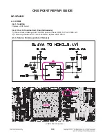
Page 47: ... board 2 3 2 How to troubleshoot Countermeasure 1 Please check soldering status of HDMI jack and check HDMI_5 1VA at IC803 pin1 2 If soldering status and 5 1 VA are abnormal replace JACK board 2 3 3 Service hint Any picture Remark JACK board top view IC803 IC803 IC800 IC800 ...

Page 48: ...Solution Replace JACK board 2 4 2 How to troubleshoot Countermeasure 1 Please check soldering status of portable jack and check IC200 pin3 VCC_5V pin4 D_3 3V 2 If portable jack and voltage has abnormal status replace JACK board 2 4 3 Service hint Any picture Remark IC200 IC200 FB202 FB202 FB203 FB203 ...

Page 49: ...P L TOP L SR L SR L CN700 pin6 5 4 3 2 1 Center Center CN701 pin2 1 and SR L SRL TOP R TOP R FR R FR R CN702 pin8 7 5 4 2 1 2 Check resistor crack cold solder of AMP IC out R718 R723 R724 R719 R7L9 R7L8 R7M1 R7M0 R722 R720 R7L5 R7H1 R7K9 R7H9 3 If AMP IC out is ok and speaker out has DC voltage replace MAIN board 3 1 3 Service hint Any picture Remark MAIN board top view CN702 CN702 CN701 CN701 CN7...

Page 50: ...lution Replace MAIN board 3 2 2 How to troubleshoot Countermeasure 1 Check PVDD voltage 20 VA of IC706 IC708 IC707 IC710 pin17 18 19 31 32 If PVDD voltage has 20 V under refer to STEP 1 1 2 Check impedance 4 Ω of speaker unit If impedance of speaker unit has 1 Ω under replace speaker unit 3 If check point 1 2 is ok replace MAIN board 3 2 3 Service hint Any picture Remark ...

Page 51: ...Replace MAIN board 3 3 2 How to troubleshoot Countermeasure 1 Check voltage 20 V of IC706 IC708 IC707 IC710 at pin17 18 19 31 32 if 12 V has problem refer to STEP 1 1 2 If 20 V is OK replace MAIN board 3 3 3 Service hint Any picture Remark MAIN board top view IC710 IC710 IC707 IC707 IC708 IC708 IC706 IC706 ...

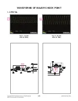
Page 52: ...3 15 1 WAVEFORMS OF MAJOR CHECK POINT 1 CRYSTAL Fig 1 2 Crystal X801 27 MHz Fig 1 1 Crystal X501 27 MHz 1 2 2 ...

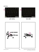
Page 53: ...3 16 CRYSTAL Fig 1 4 Crystal X601 25 MHz Fig 1 3 Crystal X603 12 288 MHz 3 4 3 4 ...

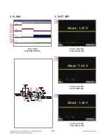
Page 54: ...5 6 2 FLASH 3 TACT KEY VCC CS CLK DO Fig 2 Flash VCC CS CLK DO 6 8 5 7 About 1 67 V Fig 3 1 Tact Key Press Power Key 9 About 1 35 V Fig 3 2 Tact Key Press FUNC Key 9 About 1 09 V Fig 3 3 Tact Key Press VOL Key 9 ...

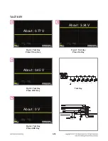
Page 55: ...18 TACT KEY About 0 77 V About 3 34 V Fig 3 4 Tact Key Press VOL Key Fig 3 7 Tact Key Press No Key Tact Key 9 9 About 0 45 V Fig 3 5 Tact Key Press Wi Fi Key 9 About 0 V Fig 3 6 Tact Key Press ADD Key 9 9 ...

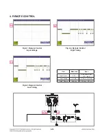
Page 56: ... Remote Control High Timing Fig 4 1 Remote Control Input Voltage 10 Fig 4 2 Remote Control Low Timing 11 12 Item Measured Spec Input Level 3 3 V IR Receiver Spec 2 7 5 5 V Low Timing 4 4 ms 3 6 ms 5 04 ms High Timing 4 48 ms 4 08 ms 5 04 ms ...

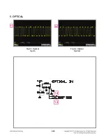
Page 57: ...3 20 13 14 5 OPTICAL Fig 5 2 Optical Opt Det Fig 5 1 Optical Opt In 13 14 ...

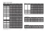
Page 58: ... IC602 Serial Flash 8 VCC 2 7 V 3 6 V 3 342 V IC705 DAC 13 21 25 47 VDD 1 14 V 1 26 V 1 215 V 20 48 DVCC 3 135 V 3 465 V 3 32 V 14 24 31 AVCC 3 135 V 3 465 V 3 32 V IC706 AMP 17 AVCC 4 5 V 26 V 20 12 V 18 19 31 32 PVCC 4 5 V 26 V 20 13 V IC708 AMP 17 AVCC 4 5 V 26 V 20 12 V 18 19 31 32 PVCC 4 5 V 26 V 20 13 V IC707 AMP 17 AVCC 4 5 V 26 V 20 12 V 18 19 31 32 PVCC 4 5 V 26 V 20 13 V IC710 AMP 17 AVC...

Page 59: ...3 24 3 23 PRINTED CIRCUIT BOARD DIAGRAMS 1 SMPS P C BOARD DIAGRAM TOP VIEW BOTTOM VIEW NOTE Warning Parts that are critical with respect to risk of fire or electrical shock ...

Page 60: ...3 26 3 25 2 MAIN P C BOARD DIAGRAM TOP VIEW ...

Page 61: ...3 28 3 27 MAIN P C BOARD DIAGRAM BOTTOM VIEW ...

Page 62: ...3 30 3 29 3 HDMI JACK P C BOARD DIAGRAM TOP VIEW BOTTOM VIEW ...

Page 63: ...3 32 3 31 4 FRONT P C BOARD DIAGRAM 5 KEY P C BOARD DIAGRAM TOP VIEW TOP VIEW BOTTOM VIEW BOTTOM VIEW ...

Page 64: ...WER ON ERROR 3 3 VA 3 V 4 7 4 WIRELESS CONNECTION 4 8 WAVEFORMS OF MAJOR CHECK POINT 4 9 1 CRYSTAL 4 9 2 FLASH MEMORY 4 9 3 VOLTAGE 4 10 4 AMP VOLTAGE 4 12 5 PWM 4 13 6 LED 4 14 CIRCUIT VOLTAGE CHART 4 15 1 ICs 4 15 2 CAPACITORS 4 15 3 CONNECTOR 4 15 PRINTED CIRCUIT BOARD DIAGRAMS 4 17 1 WOOFER SMPS P C BOARD 4 17 2 WOOFER AMP P C BOARD 4 19 3 WOOFER KEY P C BOARD 4 19 ...

Page 65: ...DIAGRAM ㇵ FFC Harness 䚌 ㇵ FFC Ha a a rness 䚌 B to B LED SMPS Wireless Wi i re e l l l l l ess 26P 0 5mm ST SMD 10P 2 5mm ST Board In KEY 3P 2mm ST DIP 3P 2mm Angle DIP KE 2P 2mm Angle DIP 2P 2mm ST DIP Bottom Top ...

Page 66: ...DC 12 V LDO 3 3V_PWM Buffer S7127F 5 VA Reset P_CTRL WL_Ready SPI Voltage Detector 5 VA P_SENSE AMP AMP SDIO_W Rear_3D SDIO_X Rear SDIO_Y Woofer RL_OUT RL_3D_OUT RR_OUT RR_OUT SW_OUT RR_3D_OUT Woofer SPK Connector Resistors OPTION Pairing S W CNT for Woofer LED CNT Rear SPK Connector DC DC 5 VA ST BY PARING STATUS LDO 5 VA 3 3V ...

Page 67: ... Fuse Bridge diode 1 1 1 Solution Replace F901 BD901 on SMPS board 1 1 2 How to troubleshoot Countermeasure 1 Look at the physical of fuse F901 2 Check the bridge diode BD901 1 1 3 Service hint Any picture Remark Woofer SMPS board top view Fuse F901 Can look at physical condition BD901 BD901 F901 F901 ...

Page 68: ... 1 2 PVDD 36 V abnormal 1 2 1 Solution Replace D951 IC901 1 2 2 How to troubleshoot Countermeasure Case 1 PVDD 36 V abnormal Check D951 and replace it Case 2 If case 1 is not problem Check IC901 and replace it 1 2 3 Service hint Any picture Remark Woofer SMPS board top view D951 D951 IC901 IC901 ...

Page 69: ...oltage then you replace woofer SMPS board 2 2 5 VA 1 Check 5 VA at WFC601 2 If 5 VA is not checked at the point then find PVDD at pin1 of WIC606 3 1 2 is NG Replace WIC606 If you can t check PVDD voltage then you replace woofer SMPS board Woofer AMP board top view Woofer AMP board top view 12 V 12 V at WFC602 at WFC602 PVDD PVDD at pin1 of WIC607 at pin1 of WIC607 PVDD PVDD at pin1 of WIC606 at pi...

Page 70: ...VA at pin7 8 of WIC603 3 Check 3 3V_PWM at WL611 nearby WIC608 4 Check 3 3V_PWM at WL615 nearby WIC601 If all voltages are OK then check the PVDD voltage of woofer SMPS board Woofer AMP board top view 3 3V_PWM 3 3V_PWM at WL615 at WL615 3 3 VA 3 3 VA at pin7 8 of WIC603 at pin7 8 of WIC603 3 3 VA 3 3 VA at WL613 at WL613 3 3V_PWM 3 3V_PWM at WL611 at WL611 ...

Page 71: ...and push Mute key sustain 3 5 sec Subwofer Push Pairing key on the back case of the wireless subwoofer The LED of of the wireless subwoofer blink red and green pull out power cord The main set and the wireless subwoofer are factory reset mode then power on Woofer KEY board top view Woofer AMP board top view 3 3 VA 3 3 VA at WL616 at WL616 Wireless module Wireless module Connection check Connection...

Page 72: ...4 9 1 4 5 2 3 WAVEFORMS OF MAJOR CHECK POINT 1 CRYSTAL 2 FLASH MEMORY VCC CS CLK DO Fig 2 Flash Memory Fig 1 Crystal WX602 24 576 MHz 1 2 3 4 5 ...

Page 73: ...4 10 7 6 3 VOLTAGE Fig 3 2 Woofer 12 VA Fig 3 1 Woofer PVDD 6 7 ...

Page 74: ...4 11 9 8 VOLTAGE Fig 3 4 Woofer 3 3V_PWM Fig 3 3 Woofer 3 3 VA 8 9 ...

Page 75: ...4 12 10 11 4 AMP VOLTAGE Fig 4 2 AMP 12 V Fig 4 1 AMP PVDD 10 11 ...

Page 76: ...4 13 13 12 5 PWM Fig 5 2 Woofer PWM SW Signal Fig 5 1 Woofer PWM SW Signal 12 13 ...

Page 77: ...4 14 14 15 6 LED Fig 6 2 Pairing On Status Green LED Fig 6 1 Pairing Off Status Red LED 14 15 ...

Page 78: ... 8 V 24 V 12 13 V WIC608 LDO 2 VIN 2 5 V 5 5 V 5 12 V 3 VOUT 1 5 V 5 V 3 312 V Test Connector Spec Connector Main Mating Connector Wireless Subwoofer WCN602 3 0 V 3 6 V 3 351 V 3 354 V Location Spec Measured V WCA603 100 uF 16 V 55 C 105 C 3 31 V WCA604 47 uF 50 V 55 C 105 C 17 75 V WCA606 47 uF 50 V 55 C 105 C 17 75 V WCA607 100 uF 16 V 55 C 105 C 3 31 V WCA608 100 uF 16 V 55 C 105 C 3 31 V WCA61...

Page 79: ...4 18 4 17 PRINTED CIRCUIT BOARD DIAGRAMS 1 WOOFER SMPS P C BOARD TOP VIEW BOTTOM VIEW NOTE Warning Parts that are critical with respect to risk of fire or electrical shock ...

Page 80: ...4 20 4 19 2 WOOFER AMP P C BOARD 3 WOOFER KEY P C BOARD TOP VIEW BOTTOM VIEW ...

Page 81: ...4 22 4 21 ...

Reviews: