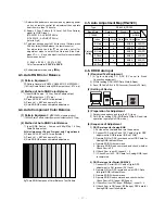
3-2. HDCP download
(1) Setting up & Confirming the G-prove
: refer to 3-1-(1) and 3-1-(2)
(2) HDCP download method
1) Click [Command -> NVRAM Write]
2) When the window of [NVRAM Write] is showed, select
“LGEKEY1.bin” to insert fill up in the File.
3) LGEKEY1 : first KEY value
4) Address : insert ‘0’
5) After finishing inputs, click the button [OK] to write
HDCP key in the EEPROM.
6) It means the end of the HDCP key download that the
message of Output terminal is showed as below.
4. SET assembly adjustment method
4-1. POWER PCB Assy Voltage Adjustments
(Va, Vs Voltage Adjustments)
(1) Test Equipment
: D.M.M 1EA
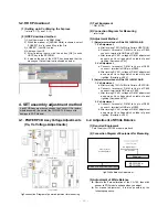
(2) Connection Diagram for Measuring
: refer to fig5
(3) Adjustment Method
1) Adjustment method ofr P/No 3501V00180A B/D
1. Va Adjustment
a. After receiving 100% Full White Pattern, HEAT RUN.
b. C terminal of D.M.M to Va pin of P805,
connect - terminal to GND pin of P805.
c. After turning RV 501, voltage of D.M.M adjustment
as same as Va voltage which on lable of panel
right/top (Deviation; ±0.5V)
2. Vs Adjustment
a. C terminal of D.M.M to Vs pin of P805,
connect – terminal to GND pin of P805.
b. After turning RV 401, voltage of D.M.M adjustment
as same as Va voltage which on label of panel
right/top. (Deviation; ±0.5V)
2) Adjustment method ofr P/No 3501V00182A B/D
1. Va Adjustment
a. After receiving 100% Full White Pattern, HEAT RUN.
b. C terminal of D.M.M to Va pin of P805,
connect - terminal to GND pin of P805.
c. After turning RV 601, voltage of D.M.M adjustment
as same as Va voltage which on lable of panel
right/top (Deviation; ±0.5V)
2. Vs Adjustment
a. C terminal of D.M.M to Vs pin of P805,
connect – terminal to GND pin of P805.
b. After turning RV 401, voltage of D.M.M adjustment
as same as Va voltage which on label of panel
right/top. (Deviation; ±0.5V)
4-2. Adjustment of White Balance
(1) Required Equipment
Color Analyzer (CA-100 or same product)
(2) Connection Diagram of Equipment for Measuring
(3) Adjustment of White Balance
O
Operate the Zero-calibration of the CA-100, then stick
sensor to PDP module surface when you adjust.
O
For manual adjustment, it is also possible by the
following sequence.
- 16 -
fig4
< 3501V00180A >
< 3501V00182A >
fig5.connection Diagram of power adjustment for measuring
Each PCB Assy must be checked by the Check JIG Set before
whole assembly. (Be careful the POWER PCB Assy not to
damage to PDP Module)
Window
MSPG-2100 or
MSTG-5200
AV Signal Input
Full Size pattern
216 gray Level
RS-232C Serial Communication
RZ/RT 50Hz
fig6 White Balance Adjustment
Summary of Contents for RT-42PX10
Page 31: ...MEMO 31 ...
Page 41: ......
Page 42: ......
Page 43: ......
Page 44: ......
Page 45: ...MAIN TOP ...
Page 47: ...April 2004 Printed in Korea P NO 3828VD0161H ...


