background image

4-4

Copyright © 2018 LG Electronics Inc. All rights reserved.

Only for training and service purposes.

DECK MECHANISM DISASSEMBLY

5. Base Up/Down

Unlock the Locking Tab (L2) in direction of arrow 
and then lift up the Base Up/Down to separate it 
from the Base Main.

Note

•  When reassembling move the Guide in direction 

of arrow (A) until it is positioned as 

Figure G-1

.

•  When reassembling insert the (B) portion of the 

Base Up/Down in the (C) portion of the Guide as 

Figure G-2

.

•  When reassembling insert the (D) portion of the 

Base Up/Down in the Hole (H2) of the Base Main 
as 

Figure G-3

.

3

2

Base Up/Down

Figure G-2

Figure G-1

(C)

(B)

Guide

Base 

Up/Down

Base Main

< Figure G >

(B)

(H2)

(A)

Figure G-3

(D)

1

(L2)

4. Pick Up Assembly

1)  Detach the Gasket Tape. 
2)  Disconnect the wires (BLK, RED, BRN, ORN) 

from the Deck PCB Assembly by desoldering. 

3) Remove the 4 screws (S2).
4)  Disconnect the FFC Cable from the Pick Up 

Assembly.

5) Remove the 4 Rubber Dampers.

3

4

(S2)

FFC Cable

Rubber 

Damper

Pick Up 

Assembly

< Bottom side view >

< Figure F >

5

BLK

RED

BRN

ORN

RED

BK

Deck PCB 

Assembly

2

1

Gasket Tape

Summary of Contents for OK75

Page 1: ...ORE SERVICING THE UNIT READ THE SAFETY PRECAUTIONS IN THIS MANUAL CONFIDENTIAL MODEL OK75 P NO AFN78511834 SEPTEMBER 2018 MODEL OK75 Copyright 2018 LG Electronics Inc All rights reserved Only for training and service purposes MINI HI FI SYSTEM ...

Page 2: ...CONTENTS SECTION 1 GENERAL SECTION 2 CABINET MAIN CHASSIS SECTION 3 ELECTRICAL SECTION 4 MECHANISM DM19D 1 1 Copyright 2018 LG Electronics Inc All rights reserved Only for training and service purposes ...

Page 3: ...UTIONS 1 5 HIDDEN KEY MODE 1 6 1 HIDDEN KEY MODE TABLE 2 HIDDEN KEY MODE DESCRIPTION PROGRAM DOWNLOAD GUIDE 1 7 FOTA UPDATE STEP USING BT APP 1 10 SPECIFICATIONS 1 12 1 2 Copyright 2018 LG Electronics Inc All rights reserved Only for training and service purposes ...

Page 4: ...solutely never be touched 4 Laser beams may damage the eyes Absolutely never permit laser beams to enter the eyes Also NEVER switch ON the power to the laser output part lens etc of the pick up if it is damaged 5 Cleaning the lens surface If there is dust on the lens surface the dust should be cleaned away by using an air bush such as used for camera lens The lens is held by a delicate spring When...

Page 5: ...e power supply lead wire from the unit 2 All equipment measuring instruments and tools must be grounded 3 The workbench should be covered with a conductive sheet and grounded When removing the laser pick up from its conductive bag do not place the pick up on the bag This is because there is the possibility of damage by static electricity 4 To prevent AC leakage the metal part of the soldering iron...

Page 6: ...atic can generate electrical charges sufficient to damage ESD devices 5 Do not use freon propelled chemicals These can generate electrical charges sufficient to damage ESD devices 6 Do not remove a replacement ESD device from its protective package until immediately before you are ready to install it Most replacement ESD devices are packaged with leads electrically shorted together by conductive f...

Page 7: ...SCRIPTION 2 1 Version Check Function Version Check Entrance Key Front Stop Remote Control Key Play for 5s Exit Key Remote Control Key Play for 1 5s Operation explanation Remote Control Key OR VFD Display Example Result MCS Version MICOM Version OPTION Version DEMO Version DJ PRO Version EQ Version EQ Check sum Version 2 2 EEPROM Initial Function Initialize data stored in EEPROM and BACKUP RAM data...

Page 8: ...n and USB2 function Caution When downloading the file you should neither unplug the USB device change to the other function nor power off the device USB device must be unplugged when the downloading process is completed ON VFD DISPLAY SCREEN 1 Fast Format USB device 2 Copy Firmware file to USB device NO USB Insert USB device at USB function SEARCH MICOM UP FINISH AUTO POWER OFF 1 7 Copyright 2018 ...

Page 9: ...B1 function and USB2 function Caution When downloading the file you should neither unplug the USB device change to the other function nor power off the device USB device must be unplugged when the downloading process is completed ON VFD DISPLAY SCREEN 1 Fast Format USB device 2 Copy Firmware file to USB device NO USB Insert USB device at USB function SEARCH FIRMWARE FINISH AUTO POWER OFF 1 8 Copyr...

Page 10: ...t USB1 function and USB2 function Caution When downloading the file you should neither unplug the USB device change to the other function nor power off the device USB device must be unplugged when the downloading process is completed ON VFD DISPLAY SCREEN 1 Fast Format USB device 2 Copy Firmware file to USB device NO USB Insert USB device at USB function SEARCH EQDEMOUP FINISH AUTO POWER OFF 1 9 C...

Page 11: ...ng the BT App with SET the user could find the Device Version info on Setting tab Step3 Select update button When touch the Update button user could update the SET firmware using FOTA Step2 Device version info When touch the Device Version info button user could find the current and latest SET version on pop up menu Step4 Confirm update Select the OK button on the caution message ...

Page 12: ... on BT App Step7 FW Flash Writing Step8 FOTA complete After completed the download from the smart phone the SET overwrite the firmware to flash memory When finishing the flash memory writing pop up message about finish is displayed and the SET auto power off Step6 Transfer FW After completed the download from server smart phone start to transfer the firmware to the SET The progress bar is displaye...

Page 13: ...UX IN 2 0 Vrms 1 kHz 0 dB 600 Ω RCA jack L R Portable in PORT IN 1 0 Vrms 3 5 mm stereo jack x 1 Microphone MIC 1 2 Sensitivity 20 mV 1 kHz 6 3 mm jack x 2 TUNER FM Tuning Range 87 5 to 108 0 MHz or 87 50 to 108 00 MHz SYSTEM Frequency Response 40 to 20 000 Hz Signal to noise ratio More than 75 dB Dynamic range More than 80 dB Bus Power Supply USB 5 V 500 mA Available Digital Input Audio Sampling ...

Page 14: ...ISASSEMBLY INSTRUCTIONS 2 2 EXPLODED VIEWS 2 9 1 CABINET AND MAIN FRAME SECTION 2 9 2 DECK MECHANISM SECTION 2 11 3 PACKING ACCESSORY SECTION 2 13 2 1 Copyright 2018 LG Electronics Inc All rights reserved Only for training and service purposes ...

Page 15: ...l rights reserved Only for training and service purposes DISASSEMBLY INSTRUCTIONS Figure 1 Panel Side L R disassembly 1 Figure 2 Panel Side L R disassembly 2 1 Remove the 6 screws 2 Disassemble each of the two screws located inside the handle ...

Page 16: ...ectronics Inc All rights reserved Only for training and service purposes Figure 3 Panel Side L R disassembly 3 Figure 4 Panel Top disassembly 1 3 Pull out Cover Side Assembly L R in the backward direction 4 Remove the 3 screws ...

Page 17: ...ed Only for training and service purposes Figure 5 Panel Top disassembly 2 Figure 6 Panel Top disassembly 3 5 Remove the two screws on the left and right sides 6 As shown in the figure remove the Panel Top by pushing the front part and lifting the rear part ...

Page 18: ...lectronics Inc All rights reserved Only for training and service purposes Figure 7 Panel Rear disassembly 7 Remove the 9 screws on the Panel Rear Figure 8 Main Set disassembly 1 8 Bracket MD Frame Main Screw 4 EA Disassembly ...

Page 19: ...s Inc All rights reserved Only for training and service purposes Figure 10 Main Set disassembly 3 10 Power Cable Disconnection Figure 9 Main Set disassembly 2 9 Remove the Set LED Connector Speaker LED Connector Speaker Network cable ...

Page 20: ...cs Inc All rights reserved Only for training and service purposes Figure 11 Main Set disassembly 4 11 Grasp both sides and pull upward to remove the assembly 12 Complete removal of the Main Set Figure 12 After detaching the Main Set ...

Page 21: ...2 8 Copyright 2018 LG Electronics Inc All rights reserved Only for training and service purposes ...

Page 22: ...260R 255 260L 266 I 269 268 267 A K MAIN I H G F C D B E J A46 263 C J N N K A 521 521 521 272 272 272 CABLE1 CN803 SMPS M M BT A51 CABLE3 B H L CABLE5 A47 RMC D CABLE2 273 274 A50 A41 262 A60 A45 F 270 TOP 251 251 A42 A52 CABLE6 CABLE6 CABLE7 275 276 261 277 259 300 A00 EXPLODED VIEWS 1 CABINET AND MAIN FRAME SECTION 2 10 2 9 ...

Page 23: ...Copyright 2018 LG Electronics Inc All rights reserved Only for training and service purposes 2 DECK MECHANISM SECTION DM19D 2 12 2 11 1049 1015 1030 A005 A00 ...

Page 24: ...ING ACCESSORY SECTION 2 13 Copyright 2018 LG Electronics Inc All rights reserved Only for training and service purposes 825 FM Wire Antenna 900 Remote Control O M AM ANT R C POWER CORD 826 Filter Ferrite Core ...

Page 25: ...2 14 Copyright 2018 LG Electronics Inc All rights reserved Only for training and service purposes ...

Page 26: ... IC502 3 35 3 SERVO IC401 3 36 4 MOTOR DRIVER IC400 3 37 5 ADC IC301 3 38 6 USB CN502 3 38 7 BLUETOOTH CN504 3 39 WIRING DIAGRAM 3 41 BLOCK DIAGRAM 3 43 CIRCUIT VOLTAGE CHART 3 45 1 IC VOLTAGE 3 45 2 FAN MOTOR VOLTAGE 3 46 3 SMPS CAPACITOR ZENER DIODE 3 46 4 MAIN CAPACITOR 3 47 5 CONNECTOR VOLTAGE 3 48 PRINTED CIRCUIT BOARD DIAGRAMS 3 53 1 SMPS P C BOARD DIAGRAM 3 53 2 MAIN P C BOARD DIAGRAM 3 57 ...

Page 27: ...rent with a digital multi meter 1 1 3 Service hint Any picture Remark F901 If F901 is not short circuit replace it with a same specifications one BD901 If BD901 is short circuit replace it with a new one TH901 or TH903 If TH901 or TH903 is open replace it with a new one L2 L1 L2 L1 L2 L1 L2 L1 5A 250V T5AL 250V CY900 VR901 SVC681 14 1 0 9 H F 1 2 FH902 1 2 CY901 GND PN901 GP390 02P TS CM901 100nF ...

Page 28: ...mally 0 2 0 3 V If it doesn t have any voltage it s destroyed Replace it with a new one 1 2 3 Service hint Any picture Remark N6 N4 N2 N7 N1 N3 N5 S1 S2 S3 P3 P2 P1 GND C952 1 2200uF 50V C953 1 2200uF 50V PC903 1 2 3 4 R951 22K 1 IC951 R954 1K C951 470P 1KVDC R955 1 8K R957 47K 1 2 R958 47K 1 2 R961 220 R952 2 2K 1 2 R962 220 R953 1K D951 SF20A400HPI C952 2200uF 63V C953 2200uF 63V R971 2K Q950 KR...

Page 29: ...VA IC202 in standby mode If there is no 12 VA check the SMPS and if doesn t appear 3 3 VA check IC202 2 Check 12 V 5 1 VA 3 3 VA DVCC_5V and DVCC_3 3V when power on the set If the set doesn t work regardless of what the KEY1 changes high to low while pressing the power button X500 and X501 work normally but if you can not power on the set replace the IC501 with a new one on the main board 2 1 3 Se...

Page 30: ... the drive signal to the transistor s Q801 2 base If the control signals from VFD DGND VDD isn t output replace VFD with a new one 3 1 3 Service hint Any picture Remark jj knukTY knuk jj rl Y zjyh h mk kv zjyh i rl Y k jj ZUZ rl Z knuk tpj vs h knuk mpsl z i thpu i rl X mk jsr tpj vs i shukpunnlhy mpsl z h thpu h k jj ZUZ tpj h mk z i rl X thpu i mpsl z i mk jsr tpj i mk XY mk kv rl Z mk XY thpu T...

Page 31: ...n3 about 3 3 V pin1 Input 5 1 VA doesn t come out check IC201 12 V from SMPS board 2 If IC201 pin2 about 5 1 V is normal check voltage of IC205 pin3 about 1 2 VA If IC205 pin3 about 1 2 VA doesn t come out check R218 R219 R221 If there s no defective component then replace IC205 3 PWR_CTRL is high check R214 R233 and if there s no defective component then check DVCC_3 3V short with GND PWR_CTRL IC...

Page 32: ...AL X500 4 2 1 Solution Replace X500 on MAIN board 4 2 2 How to troubleshoot Countermeasure 1 If 3 3 VA 1 2 VA is normal check reset High of IC501 pin T12 on MAIN board If MAIN_RESET isn t high check MICOM IC101 pin40 2 If MAIN_RESET is high check the soldering status of 24 MHz crystal X500 3 If the crystal X500 doesn t oscillate check R5B4 R5B6 C5B2 C5B5 around crystal X500 If there s no defective...

Page 33: ...1 Solution Please check and replace IC503 on MAIN board 4 3 2 How to troubleshoot Countermeasure 1 If the crystal X500 does oscillate check serial flash IC503 on MAIN board Check pin8 VCC pin6 CLK pin1 CS pin2 DO pin5 DI of below waveform 2 If pin1 2 5 6 doesn t come out check registers R5B72 5 of IC503 If registers of IC503 is OK then replace IC503 it need to download program 3 After change IC503...

Page 34: ...leshoot Countermeasure 1 Check the SPDO signal from pin16 of IC401 If no signal check DVCC_3 3V and X400 2 Check the SPIN SPIN from IC400 to CN401 for driving SPINDLE motor It is about 3 6 Vp p If no signal check M_5 V for IC400 3 Check if the FFC cable is solidly connected between CN401 and MD 4 Check the MD If the spindle motor is sort circuit or has any trouble it can not rotate CD discs Please...

Page 35: ...400 on MAIN board 5 2 2 How to troubleshoot Countermeasure 1 Check the SLDO signal from pin15 of IC401 If no signal check DVCC_3 3V and X400 2 Check the SPED SLED from IC400 to CN401 for driving SPINDLE motor It is about 2 9 Vp p If no signal check M_5 V for IC400 3 Check if the FFC cable is solidly connected between CN401 and MD 4 Check the MD If the spindle motor is sort circuit or has any troub...

Page 36: ...1 Solution Replace IC400 on MAIN board 5 3 2 How to troubleshoot Countermeasure 1 Check MOT_OPEN MOT_CLOSE signals from pin P5 L4 of IC501 to IC400 If no signal check M_5V to IC400 2 Check LOAD from IC400 to CN401 for driving the tray open close motor It is about 3 85 Vp p If no signal check M_5V to IC400 If it has any trouble replace it with a new one 3 Check if the FFC cable is solidly connected...

Page 37: ...ow to troubleshoot Countermeasure The tracking actuator makes the laser beam be positioned in the center of a track on CD disc 1 Check the TRD signal from pin14 of IC401 If no signal check DVCC_3 3V and X400 2 Check TR TR from IC400 to CN400 for driving the tracking actuator If no signal check M_5V for IC400 3 Check if the FFC cable is solidly connected between CN400 and MD 4 Check the MD If the p...

Page 38: ... How to troubleshoot Countermeasure The focusing actuator makes the laser beam keep a regular interval with the surface of a CD disc 1 Check the FDO signal from pin13 of IC401 If no signal check DVCC_3 3 and X400 2 Check F F from IC400 to CN400 for driving the focusing actuator If no signal check M_5V for IC400 3 Check if the FFC cable is solidly connected between CN400 and MD 4 Check the MD If th...

Page 39: ...als are entered to IC601 2 Check PVDD If PVDD is abnormal check the SMPS 3 Check AMP_12V for driving the gate of AMP IC a All the powers are normal but if AMP_12V is low there is possible for AMP IC to be damaged b Remove L705 L706 L707 and L708 one by one When removed a inductance if AMP_12V is recovered the IC connected to it was damaged c Replace the IC with a new one 4 Check the impedance betw...

Page 40: ...ATA2_OUT IC501_pin R2 IC601_pin26 If there is any trouble check the power for each IC The power is normal but if the signal waveform to the IC is distorted or no signal replace it with a new one 6 2 3 Service hint Any picture Remark Waveform of I2S audio interface signals IC501 D4 VDD33IO E5 VSS33IO B1 PGPA09 C1 PGPA10 C2 PGPA11 D2 PGPA12 D1 PGPA13 E1 PGPA14 E2 PGPA15 E4 PGPB00 F2 PGPB01 F1 PGPB02...

Page 41: ...the voltage is okay if so not check USB_5V to pin4 5 of CN803 2 Check USB D1 or USB D2 from MAIN board to TOP board a Check 2 0_D1 signals pin U7 U8 or 1 1_D1 signals pin A7 A8 to IC501 b Check USB signals to CN502 pin1 2 7 8 If there is any trouble check the power for IC207 The power is normal but if the signal waveform to the IC is distorted or no signal replace it with a new one 3 Check if Digi...

Page 42: ... IC301 to IC501 If no signal check AVCC_3 3V DVCC_3 3V ADC for IC301 If is NG replace it a new one 4 Check the following I2S signal flow from IC501 to IC601 Refer to Item 6 2 If there is any trouble check the power for each IC The power is normal but if the signal waveform to the IC is distorted or no signal replace it with a new one 5 Check if the digital audio AMP block is okay Refer to Digital ...

Page 43: ...h a new one 2 Check if MCS_BCK MCS_LRCK MCS_MCLK are entered from IC501 to IC201 3 Check if ADC_DATA is entered from IC301 to IC501 If no signal check AVCC_3 3V DVCC_3 3V ADC for IC301 If is NG replace it with a new one 4 Check the following I2S audio signal flow from IC501 to IC601 Refer to Item 6 2 If there is any trouble check the power for each IC The power is normal but if the signal waveform...

Page 44: ...C501 If no signal check AVCC_3 3V DVCC_3 3V ADC for IC301 If is NG replace it with a new one 4 Check the following I2S audio signal flow from IC501 to IC601 Refer to Item 6 2 If there is any trouble check the power for each IC The power is normal but if the signal waveform to the IC is distorted or no signal replace it with a new one 5 Check if the digital audio AMP block is okay Refer to Digital ...

Page 45: ...nal comes out from pin3 12 of ICA301 If no signal output check DVCC_3 3V for ICA301 replace ICA301 with a new one if it has a problem 4 Check if DSPI_BCK LRCK MCLK are entered from IC501 to IC301 Check if MIC_DATA_IN is entered from pin19 of IC301 to pin H2 of IC501 If no signal check AVCC_3 3V DVCC_3 3V for IC301 If it is abnormal change replace it a new one 5 Check the following I2S signal flow ...

Page 46: ...o signal out from module replace new module 2 Check if BT_RX TX is entered from pin6 4 of CN504 to pin L1 K1 to IC501 DSP 3 Check if MCS_BCK MCS_LRCK MIX_DATA IN is entered from IC501 to IC601 If no signal check 3 3 VA 1 2 VA for IC501 If it is abnormal change replace it a new one 4 Check the following I2S signal flow from IC501 to IC601 If there is any trouble check the power for each IC If the s...

Page 47: ... are no signal out from JK302 replace new connector and cable 2 Check if MCS_BCK MCS_LRCK MIX_DATA IN is entered from IC501 to IC601 If no signal check 3 3 VA 1 2 VA for IC501 If it is abnormal change replace it a new one 3 Check the following I2S signal flow from IC501 to IC601 If there is any trouble check the power for each IC If the signals are abnormal replace it a new one 4 Check if the digi...

Page 48: ...IC901 pin2 D902 normal YES NO Check or replace D902 Is there about 2 5 V at IC941 pin1 Replace IC941 YES YES NO D951 normal ZD932 normal Replace D951 Replace ZD932 YES NO NO D921 D922 normal Replace D921 D922 YES NO Power line of main PCB is short NO 3 23 Copyright 2018 LG Electronics Inc All rights reserved Only for training and service purposes ELECTRICAL TROUBLESHOOTING GUIDE ...

Page 49: ...ES NO Check or replace D903 Check P_CTRL HIGH signal from MCS Check PC902 Q901 normal Replace Q901 Check or replace Q911 YES NO D951 normal Replace D951 YES NO Is there about 2 5 V at IC951 pin1 Replace IC951 YES NO Q911 base HIGH Power line of main PCB is short NO NO 3 24 Copyright 2018 LG Electronics Inc All rights reserved Only for training and service purposes ELECTRICAL TROUBLESHOOTING GUIDE ...

Page 50: ...r replace LED harness cable No VFD YES VFD_12V is normal VFD_3 3V is normal VFD_CLK STB DO is normal Check or replace Q202 Q205 Check or replace Q203 Q206 Check or replace R808 R811 R814 YES YES YES NO NO NO Check or replace VFD 3 25 Copyright 2018 LG Electronics Inc All rights reserved Only for training and service purposes ELECTRICAL TROUBLESHOOTING GUIDE ...

Page 51: ...NG GUIDE 2 MCS PART CHECK YES YES YES YES YES MCS PART CHECK OK Refer to SMPS troubleshooting Check and change IC204 X501 32 768 kHz X500 24 MHz Check the operation Check and change IC202 IC205 NO NO NO Check if voltage of CN201 pin1 2 12 V Check if IC204 have DVCC_3 3V output Check if IC202 IC205 have 3 3 VA 1 2 VA output ...

Page 52: ...VH Q801 Q802 D801 D804 Check CN804 connection Check data IC501 pin C2 B3 B1 Check each pin voltage FLD light on Refer to SMPS MPEG troubleshooting Check CN201 pin1 2 12 V input voltage Check if both end voltage of FL FL are over 1 85 V VH over 29 V Check CN804 connection and DVCC_3 3V of VDD C806 Check IC501 VFD801 data communication STB DATA CLK NO NO NO NO NO YES YES YES YES YES YES ...

Page 53: ... R510 R509 OK OK OK OK Check IC601 pin21 CLK input Refer to SMPS troubleshooting Check CN201 pin1 2 12 V Check X601 12 288 MHz operation Check IC501 MLC3730 pin U13 RESET pin L14 SDA pin L13 SCL output Check X601 12 288 MHz Check IC601 input data Check IC601 Check CD Assy communication Pin22 23 24 Check IC601 TAS5548 input data pin24 PWM wave Check PWM modulator output FL Pin48 49 FR Pin46 47 Othe...

Page 54: ...ER AMP PART CHECK OK Refer to SMPS troubleshooting Check each line resistor output voltage Replace the coil Check IC701 IC702 Pin51 52 42 43 38 39 30 31 input voltage Check PWM modulator input IC701 pin4 5 IC702 pin4 5 10 11 Check IC701 IC702 pin28 29 36 37 44 45 52 53 NO NO NO Check CN201 pin1 2 12 V pin8 9 10 48 5 V 35 5 V Check IC701 IC702 pin64 AMP_12V input Check output line coil ...

Page 55: ...rposes ELECTRICAL TROUBLESHOOTING GUIDE 6 TUNER AUX FUNCTION CHECK FUNCTION CHECK Check CN201 pin1 2 12 V IC501 output data Check IC302 JK301 Replace IC501 Check IC301 Pin8 ADC_3 3V Pin13 14 DVCC_3 3V Check IC301 pin27 28 1 2 input Check IC301 pin18 output data NO NO NO NO YES YES YES YES OK ...

Page 56: ... training and service purposes ELECTRICAL TROUBLESHOOTING GUIDE 7 TUNER FUNCTION CHECK TUNER FUNCTION CHECK Check tuner data line R C Check IC301 Pin27 28 Check tuner IC IC302 voltage Pin11 AVCC_3 3V Check tuner IC302 operation NO NO YES YES YES Refer to function check ...

Page 57: ... Is the MD PN401 pin22 about 190 mV Check MD pick up IM driving Focus and tracking is ok Check Vcc of IC401 Replace IC501 Check cristal X400 Is motor ok about 12 Ω Is no signal at speaker Can the disc insert Disc reading is ok Check the signal of IC401 Check IC501 input output and control line Check the signal 16 9344 MHz at IC401 pin49 Focus tracking sled signal is ok Is load ok NO NO NO NO NO NO...

Page 58: ...UBLE USB FUNCTION USB FUNCTION Check USB jack CN801 CN802 Replace IC501 Check CN502 Check IC501 pin U7 U8 A7 A8 Display NO FILE Check USB_5V Display READ Plug in USB device Display NO USB Check USB_D D R5B69 R5B70 C5B11 C5B14 ZD505 ZD506 NO NO NO NO YES YES YES YES YES YES YES Check USB audio file in USB device MP3 WMA file is playable ...

Page 59: ...33USB20 U7 PUDP20 T8 PRTUNE20 U8 PUDN20 T9 VSS33USB20 P9 VDD12USB20 N9 VSS12USB20 U9 VDD33OSC U10 PXI U11 PXO U12 VSS33OSC T10 PDD12ALIVE T11 PTEST T12 PRESETN T13 PREMOCON PGPE 10 U13 PHUARTRX PGPE 11 P10 PGPE05 U14 PSPDIFRX PGPE 12 P11 PGPE06 T14 PEXTSRC0 PGPE 13 N11 PGPE07 T15 PEXTSRC1 PGPE 14 U15 PWAKEUP T16 U16 U17 P12 P13 7 6 B 5 R K 7 4 100 R5B59 R5B58 470 R5B48 33 R5B71 44 2 R5B52 33 R5B55...

Page 60: ... WE 17 CAS 18 RAS 19 CS 20 BS0 21 BS1 22 A10 AP 23 A0 24 A1 25 A2 26 A3 27 VDD 28 VSS 29 A4 30 A5 31 A6 32 A7 33 A8 34 A9 35 A11 36 A12 37 CKE 38 CLK 39 UDQM 40 NC 41 VSS 42 DQ8 43 VDDQ 44 DQ9 45 DQ10 46 VSSQ 47 DQ11 48 DQ12 49 VDDQ 50 DQ13 51 DQ14 52 VSSQ 53 DQ15 54 VSS R5B115 22 3 3VAA DRM_CLK DRM_CKE DRM_SEL DRM_RAS DRM_CAS DRM_WEN A15 A13 A14 A10 A00 A01 A02 A03 A04 A05 A06 A07 A08 A09 A11 A12...

Page 61: ...6 9344 MHz 10 9 11 10 9 C445 15pF C444 15pF RFGND R422 220 R423 1M X400 16 9344MHz RXI RXO 11 C424 100nF C431 100nF RFGND RFGND RFGND RFGND IC401 17 DVDD 18 MCK 19 DIN DOUT 20 R W 21 BUSY 22 SUBSYQ 23 SUBDATA 24 SUBCK 25 WFCK 26 VDD_CORE 27 DGND 28 CLK 29 CLK88 30 RESETB 31 XBUFO 32 DGND R419 33 VDD_CORE DVCC3 3V CD_RESB CD_DIN_OUT CD_SUBSYQ CD_RW CD_BUSY CD_16M CD_MCK ...

Page 62: ...for Driving SPINDLE Motor IC400 Pin11 12 17 16 13 15 12 14 18 19 16 17 C427 220uF 16V C428 100nF C415 47nF C440 100nF MGND MGND MGND IC400 1 VINFC 2 TRB_1 3 REGO 2 4 VINSL 5 REGO 1 6 FWD 7 REV 8 Vcc1 9 VOTR 10 VOTR 11 VOSL 12 VOSL 13 VOFC 14 VOFC 15 VOTK 16 VOTK 17 VOLD 18 VOLD 19 Vcc2 20 VCCD 21 VCTL 22 GND 23 VINLD 24 RESET 25 TRB_2 26 VINTK 27 BIAS 28 MUTE R416 15K R417 5 6K M_5V M_5V MOT_CLOSE...

Page 63: ...SDA 4 VINR1 VIN2P 25 MS AD 30 VINR3 VIN3P 2 VINR2 VIN2M 26 MD0 12 DGND 19 GPIO3 IntC 13 DVDD 14 IOVDD 17 BCK 18 DOUT 15 SCKI 3 3V 16 LRCK DVCC_3 3V R322 5 6K R323 5 6K R318 33 R311 2 7K R310 2 7K R305 10K R306 100 R307 100 R313 33 R312 33 R308 33 R309 33 TP301 TP311 TP302 TP313 TP310 TP304 TP312 BT_ADC_SCL DSPI_BCK DSPI_LRCK DSPI_MCLK TUNER_L TUNER_R ADC_DIR_DAT PT_L PT_R MIC_DATA_IN ADC_DATA_IN R...

Page 64: ...T 27 25 26 26 27 25 CN504 1 SDA 2 SCL 3 GND 4 TXD 5 GND 6 RXD 7 RTS 8 CTS 9 RESET 10 VDD C514 33pF C522 33pF NC C512 100nF C513 100pF C515 100pF C524 100pF C532 100pF C510 10uF C509100nF C561 10uF C508 10uF DGND DGND L507 L506 L505 L508 L502 R5B1 4 7K R5B2 4 7K TP503 TP504 TP505 TP506 TP508 TP509 TP510 BTGND TP502 TP501 3 3VA 3 3VA BT_DAT BT_TX BT_RX BT_RTS BT_CTS BT_RST BT_ADC_SCL BT Module Main ...

Page 65: ...3 40 Copyright 2018 LG Electronics Inc All rights reserved Only for training and service purposes ...

Page 66: ... ght i ng C N 106 M I C W AFER C N 301 M i com 1 I C 101 LED C TR L M i com 2 I C 111 PW M TAS5548 I C 601 SD R AM I C 502 Speaker 4pi n Speaker 3pi n C N 502 U SB Port abl e JK303 R F part M ot or I C 401 10pin 23pin MD 10pin 23pin Sparkle LED 15pin SPK LED 15pin Sparkle LED 6pin 14pin 14pin X Flash LED X Flash LED 6pin 4pin ICA301 MIC AMP DRV632 MIC2 MIC1 25pin TOP Control Board Front Board 10pi...

Page 67: ...LANDING_GEAR Party Thruster Multi Speaker Lighting Micom 1 2 48Pin Sparkle Lighting X Flash Lighting FAN MCS_CS RX TX BT_TX_RX BT_PCM_BUFFER ADC AUX IN TUNER FM FM Si4705 TUNER_L R For MIC PTB PORTABLE IN AUX_L R PTB_L R AUX MIC 1 MIC 2 IR Receiver DRV603 ADC_DATA for AUX MIC_DATA_IN ADC_DATA_IN DSPI_MCLK LRCK BCK BT_ADC_DIR_SCL ADC_DIR_DAT For RCU OK75 Total 1 000W FRONT 295W X 2CH WOOFER 410W X ...

Page 68: ...with current limiting 125 C 12 IC301 4ch Audio ADC VIN 0 3V to 3 9V AVDD 3 3V AVDD 3 31V 4ch Audio ADCs with Universal Front End Input Mux 125 C 13 IC302 TUNER VDD 3 3 6V VDD 3 3V AVDD 3 32V Tuner ic 150 C 14 IC304 OPTICAL VDD 3 3 6V VDD 3 3V AVDD 3 32V Optical 125 C 15 IC400 Motor Driver VCC1 4 3 13 2V VCC2 4 3 VCC1 VCC1 5 0V VCC2 5 0V VCC1 5 11V VCC2 5 11V 5 channel BTL Driver 150 C 16 IC401 dig...

Page 69: ...72 10 30 C904 330uF 122 30 372 10 31 C933 2200uF 12 10 12 10 32 C934 470uF 12 10 12 10 33 C952 2200uF 49 10 49 10 34 C953 2200uF 49 10 49 10 NO LOCATION NO Connector Name PIN NO PIN MANE Voltage V LOCATION NO Vin Vout 1 CN502 MAIN TOP USB 1 D2 0 01 0 01 CN803 2 D2 0 07 0 07 3 DGND 0 00 0 00 4 USB_5V 5 17 5 17 5 USB_5V 5 17 5 17 6 DGND 0 00 0 00 7 D1 0 03 0 03 8 D1 0 01 0 01 2 CN504 MAIN BT Moudle ...

Page 70: ...7 T 2 46 18 F 2 47 19 SW_PDIC 4 69 20 GND 0 00 21 CD_LD 0 02 22 MON_MPD 0 21 23 CD_VR 0 00 NO LOCATION NO Connector Name PIN NO PIN MANE Voltage V LOCATION NO Vin Vout 7 CN401 MAIN MD 1 OPEN_SW 3 29 MD 2 LO 0 00 3 CLOSE_SW 3 33 4 LO 0 01 5 GND 0 00 6 SP 2 47 7 SL 2 47 8 SP 2 47 9 SL 2 47 10 NC 0 00 8 CN701 MAIN SPK 1 SW 24 40 SPK 2 SW 24 40 3 FL 24 40 4 FL 24 40 5 FR 24 40 6 FR 24 40 9 CN106 MAIN ...

Page 71: ...12 CNS103 SPAKLING DN SPK LED 1 SPKLED_B 0 3 0 3 CNS301 2 SPKLED_G 0 3 0 3 3 SPKLED_R 0 3 0 3 4 GND 0 00 0 00 13 CNF103 FRONT FRONT 1 GND 0 00 0 00 CNF101 2 GND 0 00 0 00 3 FLASH_ BLUE_L_UP 0 3 0 3 4 FLASH_ BLUE_L_UP 0 3 0 3 5 FLASH_ RED_L_UP 0 3 0 3 6 FLASH_ RED_L_UP 0 3 0 3 7 GND 0 00 0 00 8 GND 0 00 0 00 14 CNF104 FRONT FRONT 1 GND 0 00 0 00 CNF102 2 GND 0 00 0 00 3 FLASH_ BLUE_R_UP 0 3 0 3 4 F...

Page 72: ...3 53 3 54 PRINTED CIRCUIT BOARD DIAGRAMS 1 SMPS P C BOARD DIAGRAM TOP VIEW Copyright 2018 LG Electronics Inc All rights reserved Only for training and service purposes ...

Page 73: ...MPS P C BOARD DIAGRAM BOTTOM VIEW NOTE Warning Parts that are critical with respect to risk of fire or electrical shock Copyright 2018 LG Electronics Inc All rights reserved Only for training and service purposes ...

Page 74: ...Copyright 2018 LG Electronics Inc All rights reserved Only for training and service purposes 3 57 3 58 2 MAIN P C BOARD DIAGRAM TOP VIEW ...

Page 75: ...Copyright 2018 LG Electronics Inc All rights reserved Only for training and service purposes 3 59 3 60 MAIN P C BOARD DIAGRAM BOTTOM VIEW ...

Page 76: ...Copyright 2018 LG Electronics Inc All rights reserved Only for training and service purposes 3 61 3 62 3 TOP P C BOARD DIAGRAM TOP VIEW ...

Page 77: ...Copyright 2018 LG Electronics Inc All rights reserved Only for training and service purposes 3 63 3 64 TOP P C BOARD DIAGRAM BOTTOM VIEW ...

Page 78: ...Copyright 2018 LG Electronics Inc All rights reserved Only for training and service purposes 3 65 3 66 4 JACK RMC P C BOARD DIAGRAM TOP VIEW BOTTOM VIEW ...

Page 79: ...ht 2018 LG Electronics Inc All rights reserved Only for training and service purposes 3 67 3 68 5 SPARKLE LED UP P C BOARD DIAGRAM 6 SPARKLE LED DOWN P C BOARD DIAGRAM TOP VIEW TOP VIEW BOTTOM VIEW BOTTOM VIEW ...

Page 80: ...rights reserved Only for training and service purposes 3 69 3 70 7 X FLASH LED UP LEFT P C BOARD DIAGRAM 9 SPEAKER LED P C BOARD DIAGRAM 8 X FLASH LED UP RIGHT P C BOARD DIAGRAM TOP VIEW TOP VIEW BOTTOM VIEW TOP VIEW BOTTOM VIEW BOTTOM VIEW ...

Page 81: ...Copyright 2018 LG Electronics Inc All rights reserved Only for training and service purposes 3 71 3 72 ...

Page 82: ...op 4 2 2 Clamp Assembly 4 2 2 1 Plate 4 2 2 2 Magnet 4 2 2 3 Clamp 4 2 3 Tray Disc 4 3 4 Pick Up Assembly 4 4 5 Base Up Down 4 4 6 Belt Loading 4 5 7 Gear Pulley 4 5 8 Gear Loading 4 5 9 Guide 4 5 10 Deck PCB Assembly 4 5 11 Motor Assembly 4 5 12 FFC Cable 4 5 DECK MECHANISM EXPLODED VIEW DM19D 4 6 SECTION 4 MECHANISM DM19D CONTENTS ...

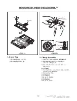
Page 83: ...ly 1 Place the Clamp Assembly as Figure B 2 Bending the Cover Top in direction of arrow 2 as Figure B 3 Separate the Clamp Assembly from the Cover Top 2 1 Plate 1 Turn the Plate to a counterclockwise direction and then lift up the Plate 2 Remove the Plate 2 2 Magnet Remove the Magnet 2 3 Clamp Remove the Clamp 1 2 S1 Cover Top Figure A Figure B Clamp Assembly 1 Clamp Assembly Plate Magnet Clamp 2 ...

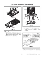
Page 84: ... separated from the MD Sub Assembly completely Note When reassembling place the Guide as Figure E MD Sub Assembly Figure D 3 1 1 2 2 Tray Disc Tray Disc Figure E Guide 3 Tray Disc 1 Insert and push a flat head screwdriver in the Emergency eject hole H1 at the right side so that the Tray Disc is ejected about 15 20 mm 2 Pull the Tray Disc until it is locked Bottom side view Tray Disc Tray Disc Figu...

Page 85: ...the C portion of the Guide as Figure G 2 When reassembling insert the D portion of the Base Up Down in the Hole H2 of the Base Main as Figure G 3 3 2 Base Up Down Figure G 2 Figure G 1 C B Guide Base Up Down Base Main Figure G B H2 A Figure G 3 D 1 L2 4 Pick Up Assembly 1 Detach the Gasket Tape 2 Disconnect the wires BLK RED BRN ORN from the Deck PCB Assembly by desoldering 3 Remove the 4 screws S...

Page 86: ...Separate the Guide from the Base Main 10 Deck PCB Assembly 1 Disconnect the wires RED BK form the Deck PCB Assembly by desoldering 2 Remove the 1 screw S3 3 Separate the Deck PCB Assembly from the Base Main 11 Motor Assembly Unlock the Locking Tab L4 in direction of arrow and then separate the Motor Assembly from the Base Main 12 FFC Cable Remove the FFC Cable Gear Pulley Belt Loading Deck PCB Ass...

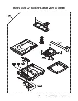
Page 87: ...4 6 Copyright 2018 LG Electronics Inc All rights reserved Only for training and service purposes DECK MECHANISM EXPLODED VIEW DM19D 1049 1015 1030 A005 A00 ...

Reviews: