


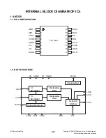
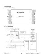


3-38
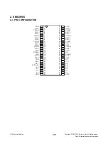
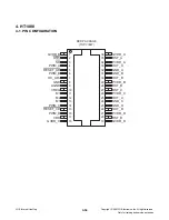
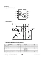
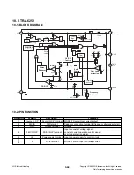
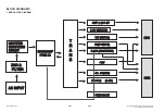
6. KS24L161
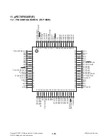
6-1. PIN CONFIGURATION
Vcc
A0
WP
A1
SCL
A2
SDA
Vss
KS24L161
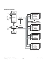
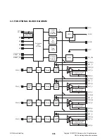
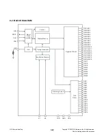
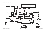
6-2. BLOCK DIAGRAM
SDA
Start/Stop
Logic
Control Logic
HV Generation
Timing Control
Word Address
Pointer
Row
Decoder
EEPROM
Celt Array
2,048 x 8 Bits
Column Decoder
Data Register
D
OUT
and ACK
Slave Address
Comparator
WP
SCL
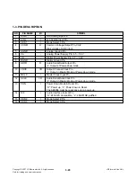
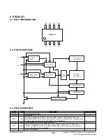
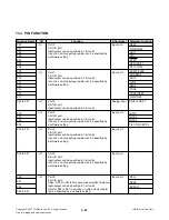
6-3. PIN DESCRIPTION
Name
Type
Description
Circuit Number
A0, A1,A3
-
No internal connection
-
V
SS
-
Ground pin.
-
Bi-directional data pin forthe I
2
C-bus serial data interface. Schmitt tigger input and
SDA
I/O
open-drain output. An external pull-up resistor must be connected to V
DD
. Typical values
3
for this pull-up resistor are 4.7K
Ω
(100kHz) and 1K
Ω
(400kHz).
SCL
Input
Schmitt tigger input pin for serial clock input.
2
Input pin for hardware write protection control. If you tie this pin to V
CC
, the write
WP
Input
function is disabled to protect previously written data in the entire memory; if you tie it
1
to V
SS
, the write function is enabled.
V
CC
-
Single power supply.
-
Copyright © 2007 LG Electronics. Inc. All right reserved.
Only for training and service purposes
LGE Internal Use Only