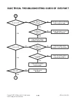
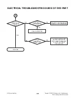
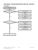


3-33
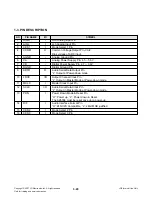
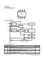
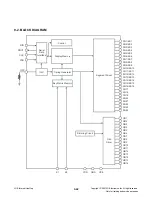
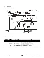
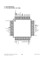
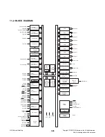
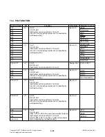
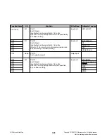
3-3. PIN DESCRIPTION
Pin
Description
A0-A19
20 Addresses
DQ0-DQ14
15 Data Inputs/Outputs
DQ15/A-1
DQ15 (Data Input/Output, Word Mode)
A-1 (LSB Address Input, Byte Mode)
CE#
Chip Enable
OE#
Output Enable
WE#
Write Enable
RESET#
Hardware Reset Pin, Active Low
BYTE#
Selects 8-bit or 16-bit mode
RY/BY#
Ready/Busy Output (N/A SO 044)
Vcc
3.0 volt-only single power supply
(see Product Selector Guide for speed options and voltage supply tolerances)
Vss
Device Ground
NC
Pin Not Connected Internally
Copyright © 2007 LG Electronics. Inc. All right reserved.
Only for training and service purposes
LGE Internal Use Only