- 44 -
LGE Internal Use Only
Copyright © 011 LG Electronics. Inc. All right reserved.
Only for training and service purposes
3. TECHNICAL BRIEF
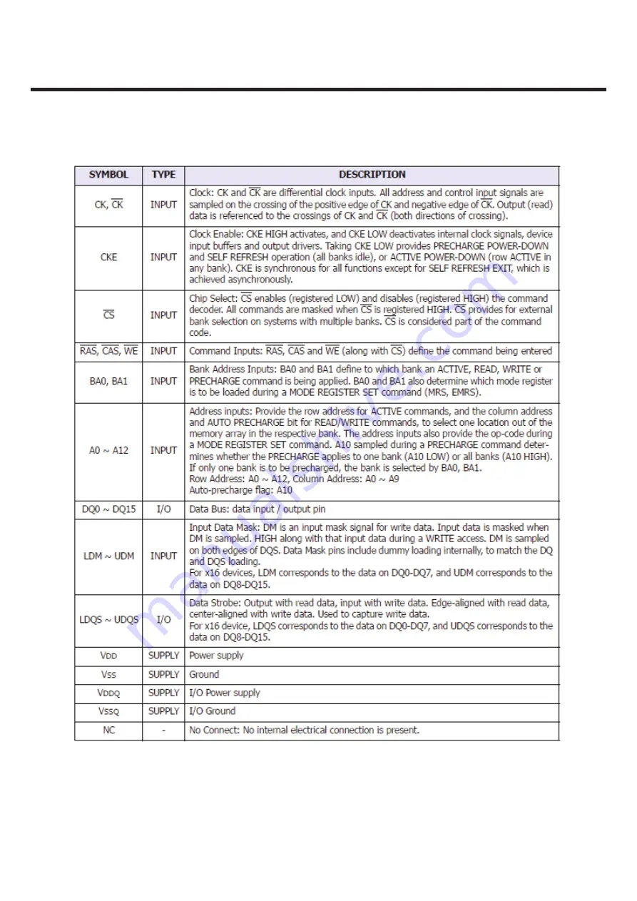
Table 3.7.1 DDR SDRAM PIN Description Table
Page 1: ...Internal Use Only Service Manual LG A258 Date June 2011 Issue 1 0 ...
Page 2: ...3 15 Camera Interface 61 3 16 KEY BACLKLIGHT LED Interface 63 4 TROUBLE SHOOTING 64 4 1Trouble shooting test setup 64 4 2 RF Component 65 4 3 RXTrouble 66 4 4TXTrouble 72 4 5 Power OnTrouble 78 4 6 ChargingTrouble 81 4 7VibratorTrouble 84 4 8 LCDTrouble 87 4 9 CameraTrouble 91 4 10 SpeakerTrouble 94 4 11 EarphoneTrouble 97 4 12 Micro SDTrouble 102 4 13 BluetoothTrouble 104 4 14 FM RadioTrouble 106...
Page 3: ...facilities accessed through or connected to it The manufacturer will not be responsible for any charges that result from such unauthorized use B Incidence of Harm If a telephone company determines that the equipment provided to customer is faulty and possibly causing harm or interruption in service to the telephone network it should disconnect telephone service until repair can be done A telephone...
Page 4: ...ation Phone may interfere with sensitive laboratory equipment medical equipment etc Interference from unsuppressed engines or electric motors may cause problems H Electrostatic Sensitive Devices ATTENTION Boards which contain Electrostatic Sensitive Device ESD are indicated by the sign Following information is ESD handling Service personnel should ground themselves by using a wrist strap when exch...
Page 5: ...iate Frequency IF International Portable User Identity IPUI Global System for Mobile Communications GSM General Purpose Interface Bus GPIB Gaussian Minimum Shift Keying GMSK Flexible Printed Circuit Board FPCB Electrostatic Discharge ESD Electrical Erasable Programmable Read Only Memory EEPROM Digital Signal Processing DSP dB relative to 1 milli watt dBm Digital Communication System DCS Digital to...
Page 6: ... Transmitter UART Time Division Multiple Access TDMA Time Division Duplex TDD Travel Adapter TA Side Tone Masking Rating STMR Pseudo SRAM PSRAM Static Random Access Memory SRAM Sending Loudness Rating SLR Subscriber Identity Module SIM Surface Acoustic Wave SAW Real Time Clock RTC Root Mean Square RMS Receiving Loudness Rating RLR Radio Frequency RF Public Switched Telephone Network PSTN Phase Loc...
Page 7: ... Approx 3 hours TX output power GSM EGSM 33dBm Level 5 DCS PCS 30dBm Level 0 SIM card type 3V Small Display MAIN 2 2 TFT 176 Ý 220 pixel 262K Color Sub 0 968 mono 96 x 64 Status Indicator Button Outside Send Key End Key Navi Key 4EA OK Key Menu Key Contacts Key Button Inside Numeric Key 12EA ANT Internal EAR Phone Jack 5PIN I O PC Synchronization Yes Speech coding EFR FR HR AMR Data and Fax Yes GP...
Page 8: ...s Inc All right reserved Only for training and service purposes 2 PERFORMANCE Travel Adapter Yes Speaker Receiver 18x12Ȱ Speaker Receiver MIDI SW MIDI Mono SPK Item Feature Comment Camera 1 3M Bluetooth FM Radio Bluetooth version 2 1 76 108MHz supported ...
Page 9: ...r Level Level Power Toler Level Power Toler 6 31dBm 3dB 14 15dBm 3dB 7 29dBm 3dB 15 13dBm 3dB 8 27dBm 3dB 16 11dBm 5dB 9 25dBm 3dB 17 9dBm 5dB 10 23dBm 3dB 18 7dBm 5dB 11 21dBm 3dB 19 5dBm 5dB 12 19dBm 3dB GSM850 EGSM 5 33dBm 2dB 13 17dBm 3dB Level Power Toler Level Power Toler 1 28dBm 3dB 9 12dBm 4dB 2 26dBm 3dB 10 10dBm 4dB 3 24dBm 3dB 11 8dBm 4dB 4 22dBm 3dB 12 6dBm 4dB 5 20dBm 3dB 13 4dBm 4dB ...
Page 10: ...Bc 100 0 5 200 30 250 33 400 60 600 1 200 60 1 200 1 800 60 1 800 3 000 63 3 000 6 000 65 6 000 71 GSM850 EGSM Offset from Carrier kHz Max dBc 100 0 5 200 30 250 33 400 60 600 1 200 60 1 200 1 800 60 1 800 3 000 65 3 000 6 000 65 6 000 73 DCS PCS 6 Output RF Spectrum due to switching transient GSM850 EGSM Offset from Carrier kHz Max dBm 400 19 600 21 1 200 21 1 800 24 Item Description Specificatio...
Page 11: ... transient Offset from Carrier kHz Max dBm 400 22 600 24 1 200 24 1 800 27 7 Spurious Emissions Conduction Emission Status 8 Bit Error Ratio GSM850 EGSM BER Class II 2 439 102 dBm DCS PCS BER Class II 2 439 102 dBm 9 RX Level Report Accuracy 3 dB 10 SLR 14 3 dB 11 Sending Response 300 12 1 000 6 2 000 6 3 000 6 Frequency Hz Max dB Min dB 100 200 4 000 3 400 9 0 0 4 4 12 0 0 4 12 RLR 4 3 dB DCS PCS...
Page 12: ...0 2 2 14 STMR Over 17 dB Mean that Adopt a straight line in between 300 Hz and 1 000 Hz to be Max level in the range 15 Stability Margin 6 dB 20 10 0 7 dB to ARL dB Level Ratio dB 35 30 10 30 7 33 3 33 7 31 7 17 5 22 5 25 5 16 Distortion 17 Side Tone Distortion Three stage distortion 10 18 System frequency 26 MHz tolerance 2 5 ppm 19 32 768KHz tolerance 30 ppm 20 Ringer Volume At least 58 dB SPL u...
Page 13: ...ge Warning Blinking Bar 25 Forced shut down Voltage 3 35 0 05V 27 Battery Type Lithium Ion Battery Standard Voltage 3 7 V Battery full charge voltage 4 2 V Capacity 900mAh 28 Travel Charger Switching mode charger Input 100 240V 50 60 Hz Output 5 1V 400 mA 26 Sustain RTC without battery Over 30 sec 7 7 5 5 4 92 Over 93 2 1 0 106 2 It alarms 3 times standby 10 1st warning 5 2nd warning 0 3rd warning...
Page 14: ... ELW 986 75 16 9 5 60 5 6 4Z 2 5 B5 B1 3 B5 B1 3 1 1 ODVK ELW 1 1 00 0 025 86 8 57 SLQ RQQ A 6 0 1 57 4 08 KDUJLQJ ULYLQJ 5 6 5 0 0ELW 7 6 5 0 3 0 8 57 8 57 HDGVHW 0B 17 5 ULYLQJ 2 8 57 7 5 86 6 3 0 86 6 A 6 XGLR 6XE 6 VWHP 308 63 86 6 3 0 6 0LF 1 0 5DGLR 6 63 6 03 0 6 0 5 2 73 3 308 63 5 9 03 0 5 0 5 2 5 0LF 1 6 0 5 2 P K L LRQ KDUJLQJ 3 1 LG A258 Functional Block Diagram The functional component...
Page 15: ...t Earpiece Charge Pump negative voltage for bipolar audio out VMMC VANA LPMU VUSB LAUX Charge DC DC Buck Vibrator 64 bit bus 32 bit bus IF GMSK DAC SD PLL FEM 32 kHz XO DSP ADC PA c s i M Low Power DCXO RF PMU USB 2 0 FS CIF DCC Keypad 4k 7 0 15 5 1 8V 2 5V VCHARGE 4 5 V 20V 2 T A B V N E S N E S P E S N E S S C C S B G H C D D V T N H S V BC 847 S 1 2 6 4 5 3 for example ZXTP 25020 min 10 µF 0 V ...
Page 16: ... possible with external circuitry Fully integrated digital controlled X0 Additional buffer for 2 external system clocks Fully digital RF Synthesizer incl ȭȟ Transmitter 3 2 3 Baseband DSP 178 MHz TeakLite MCU ARM 1176 208 MHz MCU RAM 3 00Mbit Memory I F 1Gbit NOR flash One NAND flash SDR SDRAM 4Gbit NAND flash DDR SDRAM Modem GPRS class 12 RX TX CS1 CS4 EGPRS class 12 RX MCS1 MCS9 TX MCS1 MCS4 Cip...
Page 17: ...it ECC supported Parallel Flash Cellular RAM Page Burst Mode 16 bit AD multiplexed concurrent usage of DDR interface and AD multiplexed interface is not supported 16 bit AAD multiplexed iNAND Type e g oneNAND SDRAM DDR SDRAM up to 4 Gbit SDR SDRAM up to 1 Gbit Memory card SD MMC card interface with 1 or 4 data lines 3 2 5 Connectivity Up to 3xUSIF configurable either as SPI or UART I2C I2S Interfa...
Page 18: ...l microphone supported Differential microphone input 3 2 7 FM Radio Integrated FM radio FM Stereo RDS Receiver Sensitivity 2 ɆV EMF Support for US EU bands Stereo recording 3 2 8 Power Management Direct to Battery Connection LDOs incl capless DC DC step down converter DC DC step up for white LED supply Battery Type Li Ion Charging control Battery temperature Watchdog protection Start up on flat ba...
Page 19: ... post processing Scaling Rotation 90 steps Mirroring Overlay with alpha blending Color conversion YUV RGB 2D vector graphics Lines filled rectangles Bit block transfer e g sprites scrolling antialiased bitmap fonts 3 2 10 Camera 2 Mpx YUV parallel interface HW JPEG encoder 39 Mpx sec 39 MHz Pixel Rate 15 fps 2 Mpx full resolution 3 2 11 Video Capabilities Video Decoding MPEG 4 H 263 QCIF 30 fps QV...
Page 20: ...wer for a typical standard phone Figure 3 2 1 Block Figure of the PMU Modules X Gold tm 215 DC DC Step Down Converter for 1 8V SD1 The DC DC converter generates a 1 8V supply rail This voltage rail is used to supply main parts of the system like the digital core of the chip via LDO LCORE some parts of the mixed signal macro parts of the RF macro and the external memory if a 1 8V memory is used The...
Page 21: ... supply for the USB transceiver output driver and input If no USB interface is required LUSB can be used as general purpose LDO LAUX The LAUX generates VAUX It is a general purpose LDO and can be used for different functions depending on the phone application e g for the display or Camera LMMC The LMMC generates VMMC It is a general purpose LDO and can be used e g for memory cards LSIM The LSIM LD...
Page 22: ... 22 LGE Internal Use Only Copyright 2011 LG Electronics Inc All right reserved Only for training and service purposes 3 TECHNICAL BRIEF Table 3 3 1 Power supply Domains without RF ...
Page 23: ...rs the SYSTEM OFF state and only continuous the startup procedure if a switch on event like first connect on key wake up or charge detect occurs PMU main State Machine The main PMU state machine is always connected to VPMU also The power up sequence driven by the PMU state machine can be seen in Figure18 After enabling the reference HPGB and waiting for the settling time the battery voltage is mea...
Page 24: ...RGE or VDDRTC as input voltage The input voltage is selected automatically by a bulk switch circuit LADC the ADC and the oscillator are enabled on request for every battery measurement if the charger unit is not running This is handled by an ADC control block in one of the state machines If the charger unit is running the ADC is controlled by the charger state machine Figure 3 3 2 First Part of th...
Page 25: ...HNICAL BRIEF 25 LGE Internal Use Only Copyright 2011 LG Electronics Inc All right reserved Only for training and service purposes Figure 3 3 3 Second Main Part of the Startup State Machine in the VPMU Domain ...
Page 26: ...switched on 3 3 5 Switching on due to charging When a battery with a voltage below the SSONLEV level is inserted the state machine will not start the system As long as the battery voltage stays lover than SYSONLEV the system will stay off The only possibility to start up the system is due to an external charger If an external charger is connected and detected and the battery is charged above the S...
Page 27: ... ups a staggered turn on approach for the regulators is implemented The regulators are turned on in a well defined sequence thus spreading the in rush current transients over time The IO s of X GOLD TM 215 are isolated in OFF mode core supply is off The isolation signal is controlled by the PMU state machine This ensures that the PADs are in a well defined state during core supply settling This al...
Page 28: ... 28 LGE Internal Use Only Copyright 2011 LG Electronics Inc All right reserved Only for training and service purposes 3 TECHNICAL BRIEF Figure 3 3 4 Start Up Sequence triggered by First Connect Event ...
Page 29: ...nal controls for example the ɆC subsystem and releases reset for the controller During normal start up the PMU releases the reset_pmu_n_o signal after entering the SYSTEM ON state At this time the resetout_o signal is high the RESET_N pad is not pulled low and therefore the reset_postscu_n_o signal follows the reset_pmu_n_o signal That means the ɆC reset will be released and the ɆC starts operatio...
Page 30: ...the PMU enables the DCXO After the system is running the DCXO is controlled by the SCU of the baseband by using the vcxo_enable signal This is handled by a dedicated logic in the PMU see Figure 3 3 6 As long as rf_sysclk_en_pmu the output of the PMU state machine is high vcxo_enable controls the rf_sysclk_en signal to the RF If rf_sysclk_en_pmu is low the DXCO is switched off independent from vcxo...
Page 31: ...s Routed in the PMU 3 3 11 PMU Clock During the first startup for example plugging in a battery a PMU internal oscillator is used for generation of the PMU clock pmu_clock The frequency is slightly above 32 kHz typ 50 kHz to be out of the audio band also for worst case devices After first startup the software shall enable the 32 kHz crystal oscillator It is not possible to use the 32 kHz oscillato...
Page 32: ...ble 3 3 13 DC DC Pre Load Register Handling The DC DC converter works in different modes If the mode is switched from PFM to PWM the pulse width of the DC DC converter depends on the current battery voltage and on the output voltage The PMU state machine knows the battery voltage because of the battery supervision function Depending on this value it selects a startup pulse width for the DC DC conv...
Page 33: ...ulti slot operation The module consists of a GSM850 900 PA block and a DCS1800 PCS1900 PA block Impedance matching circuitry for 50 ohm input and output impedances Tx harmonics filtering high linearity low insertion loss RF switch and a Power Amplifier Control PAC block with internal current sense resistor The two Hetero junction Bipolar Transistor HBT PA blocks a BiFET PAC and switch control circ...
Page 34: ...GSM850 900 PA block and a DCS1800 PCS1900 PA block Impedance matching circuitry for 50 ohm input and output impedances Tx harmonics filtering high linearity low insertion loss RF switch and a Power Amplifier Control PAC block with internal current sense resistor The two Hetero junction Bipolar Transistor HBT PA blocks a BiFET PAC and switch control circuit are fabricated onto a single Gallium Arse...
Page 35: ... T A B V 2 T T A B V 3 D N G 4 D N G 5 D N G 6 D N G 7 D N G 2 x R 3 D V S R 1 x R D V S R N E x T P M A R V 8 D N G GND9 GND10 ANT GND11 GND12 GND13 PGND SW300 2 G T N A F R 1 G 33p C322 FL300 10 5 3 2 6 4 7 8 9 1 I1 O1 1 O1 2 O2 1 I2 O2 2 1 G 2 G 3 G 4 G VBAT L309 22 L308 47p 1 5n L310 1 2p C333 DNI L305 1K R303 1 2n L306 39p C320 C310 15n DNI C330 2 2u C335 100n L307 33p C334 L313 47p 1p C309 1...
Page 36: ...scillator External Connection Reference frequency is generated by a digitally adjustable 26 MHz oscillator designed for 8 pF crystals This frequency serves as comparison frequency within the RF PLL and as clock frequency for the digital circuitry The reference clock can also be applied to external components like Bluetooth or GPS via two independently controllable FSYS output pins ...
Page 37: ...Block DIAGRAM of RF Subsystem Multi Modulus Divider TDC L z 2 4 SER RF Subsystem Integrated 3 8GHz DCO 26 MHz TX1 850 900MHz TX2 1800 1900MHz CTRLEN CTRLDA CTRLCLK SYSCLK_EN FSYS1 FSYS2 VRAMP VDET XOX XO t r a P B B U M P Ramp DAC DigRF 3 Wire Bus ADC 4 2 RXTXEN RXTXDA PAEN PABS FE1 FE2 PAR D M M D D V C D T D D V 1 3V LPF LPF RX12 RX12X 850 900MHz RX34 RX34X 1800 1900MHz DCOC DCOC ADC ADC S M D D...
Page 38: ...requency dividers by 2 4 the LO frequency is derived from the RF frequency synthesizer The receive path is fully differential to suppress the on chip interferences and reduce DC offsets The analog chain of the receiver contains two LNAs low high band a quadrature mixer followed by an analog baseband filter and 14 bit continuous time delta sigma analog to digital converter The filtered and digitize...
Page 39: ... synthesizer is used as modulation loop to process the phase frequency signal The 26 MHz reference signal of the phase detector incorporated in the PLL is provided by the reference oscillator 3 6 2 3 Front end PA Control Interface Two outputs FE1 FE2 for direct control of antenna switch modules enable to select RX and TX mode as well as low and high band operation An extra band select signal PABS ...
Page 40: ...NC20 NC21 NC9 NC19 NC8 NC11 NC12 NC17 NC18 NC7 NC16 NC25 NC6 NC10 NC5 NC13 NC14 NC4 NC2 NC24 NC22 NC23 NC15 NC3 VCC1 VCC2 VSS1 VSS4 VSS8 VSSQ5 VSSQ4 VSSQ9 VSSQ8 VSSQ3 VSS2 VSS3 VSSQ10 VSSQ1 VSSQ2 VSS5 VSSQ6 VSSQ7 VSS6 VSS7 A0 A1 A2 A3 A4 A5 A6 A7 A8 A9 A10 A11 A12 BA0 BA1 DQ0 DQ1 DQ2 DQ3 DQ4 DQ5 DQ6 DQ7 DQ8 DQ9 DQ10 DQ11 DQ12 DQ13 DQ14 DQ15 CK CK CKE CS RAS CAS WED UDQM LDQM UDQS LDQS IO0 IO1 IO2 ...
Page 41: ... Array 1 K 32 Words x 64 pages x 1024 blocks Page Size 1 K 32 spare Words Block Size 64 K 2 K spare Words Page Read Program Random access 25us max Sequential access 45ns min Page program time 200us typ COPY BACK PROGRAM MODE Fast page copy without external buffering FAST BLOCK ERASE Block erase time 2 0ms typ STATUS REGISTER DATA RETENTION 100 000 Program Erase cycles with 1bit 528byte ECC 10 year...
Page 42: ...in The on chip Program Erase Controller automates all program and erase functions including pulse repetition where required and internal verification and margining of data The modify operations can be locked using the WP input The chip supports CE don t care function This function allows the direct download of the code from the NAND Flash memory device by a microcontroller since the CE transitions...
Page 43: ...hitecture two data transfer per clock cycle x16 bus width Supply Voltage VDD VDDQ 1 7 1 95 V Memory Cell Array 8Mb x 4Bank x 16 I O Bidirectional data strobe DQS Input data mask signal DQM Input Clock Differential Clock Inputs CK CK MRS EMRS JEDEC Standard guaranteed CAS Latency Programmable CAS latency 2 or 3 supported Burst Length Programmable burst length 2 4 8 with both sequential and interlea...
Page 44: ... 44 LGE Internal Use Only Copyright 2011 LG Electronics Inc All right reserved Only for training and service purposes 3 TECHNICAL BRIEF Table 3 7 1 DDR SDRAM PIN Description Table ...
Page 45: ...radio transceiver that has been optimized for use in 2 4GHz Bluetooth Wireless systems It has been designed to provide low power robust communications for applications Operating in the globally available 2 4GHz unlicensed ISM band It is fully compliant with the Bluetooth Radio Specification and enhanced data rate specification and meets or exceed the requirement to provide the highest communicatio...
Page 46: ...some integrated filtering no external filters are requires for meeting Bluetooth and regulatory harmonic and spurious requirements For integrated mobile handset applications where Bluetooth is integrated next to the celluar radio minimal external filtering can be applied to achieve near thermal noise levels for spurious and radiated noise emissions Using a highly linearized temperature compensated...
Page 47: ...cessor XMM2130 provides SIM Interface Module The XMM2130 checks status Periodically During established call mode whether SIM card is inserted or not but it doesn t check during deep sleep mode In order to communicate with SIM card 3 signals SIM_DATA SIM_CLK SIM_RST SIM interface scheme is shown in Figure 3 9 1 SIM_DATA SIM_CLK SIM_RST ports are used to communicate with Main Chip AGR NAND J200 9 8 ...
Page 48: ...62K colors LCD Driver IC ILI9225B 1 chip for Gate Source Driver Interface 8bit 16bit CPU interface Backlight 3 White LED 1 way Standby Still Moving mode display Low power consumption driving Mobile Phone Application 470n C354 DNI R317 1V8_VDD R318 100K 2 2u C341 C344 0 022uF VA300 120p C337 0 1u C340 120p C338 CAM_DVDD CN300 28 27 29 26 30 25 31 24 32 23 33 22 34 21 35 20 36 19 37 18 38 17 39 16 4...
Page 49: ...PWM signal which generated by hardware itself via register control direct connect to the VIB and VSSVIB pin from XMM215 without any external component required it is capable to driver the vibrator motor up to 150mA Figure 3 11 1 Vibrator Driver Block Diagram Figure 3 11 2 Vibrator Driver Block Vibrator Driver VIB VSSVIB C144 1u 68n L101 R127 0 C147 33p VIB_P F_VIB_P ...
Page 50: ...gh voltage headroom for maintaining constant brightness Figure 3 12 1 RT8966GQW CIRCUIT DIAGRAM 3 12 MINI ABB Interface The RT8966 is an analog subsystem which includes a linear charger 4 LDOs a 4 CH current source and a multiplexer for USB UART microphone stereo and audio on a single mini micro USB connector CAM_AVDD DNI C252 2 2u C230 5 0 2 B F 0 0 6 CAM_IOVDD 600 FB202 10K R242 VBAT 1V8_VDD 100...
Page 51: ...e as shown in the control register address tables CHG_Ctrl1 and CHG_Ctrl2 The CV mode voltage is fixed at 4 2V The pre charge threshold is fixed at 2 6V If the battery voltage is below the pre charge threshold the RT8966 charges the battery with a trickle current until the battery voltage rises above the pre charge threshold The RT8966 is capable of being powered up from AC adapter and USB Univers...
Page 52: ...s I2C to control the switch position and read the results of the accessory detectioicro USB connecn The RT8966 can also detect USB chargers including dedicated chargers D D shorted and high power host hub chargers Switches The RT8966 provides a multiple input multiplexer to support USB high Speed UART stereo audio mono audio and a microphone The output of the multiplexer is used to connect to a mi...
Page 53: ...e reduces the power consumption The module is able to debounce and scan the external keypad matrix automatically without any software intervention After debouncing it generates an interrupt The interface controller contains information about the key or key combination that was pressed and how long it was pressed 150 R215 KB214 150 R216 150 R218 150 R220 KB204 KB203 KB208 KB211 KB209 KB210 VA209 15...
Page 54: ...terface 32 768 kHz sample clock Debouncing process 0 to 100 ms 10 ms resolution duration programmable by controller Module sends an interrupt whenever a change occurs Up to 8 rows and 8 columns of a standard keypad matrix possible Up to 8 additional keys connected to ground possible Pressed key or combination of pressed keys and duration 0 to 1 s 10 ms resolution stored within keypad registers Res...
Page 55: ...sequently It features a high quality stereo digital to analog path with amplifier stages for connecting acoustic transducers to X GOLD 215 In audio in path the supply voltage generation for electret microphones a low noise amplifier and analog to digital conversion are integrated in X GOLD 215 A more detailed functional description will be given in the following sections The audio front end itself...
Page 56: ...modified by certain control register settings Due to the new gain settings in the TX path the maximum input voltage is limited to 0 8 Vpp In both voiceband paths the value range for voice samples is confined to 97 5 i e to 31948 31947 or 8334H 7CCBH in X GOLD 215 On the TX path 83 1 s on the VTPDM line correspond to a 16 bit value of 7CCBH and 17 1 s correspond to a 16 bit value of 8334H at the di...
Page 57: ... The DAC outputs can be switched to several output buffers In audio in section there is an input multiplexer which selects either one of two differential microphone inputs to be connected to the low noise amplifier and analog pre filter The signals from the analog pre filter are input to a second order sigma delta analog to digital converter In addition there is a connection for FM radio playing A...
Page 58: ...n work unipolar mode where an AC coupling of the headset might be needed or can work also in bipolor mode The differential loudspeaker driver can be used to drive a 8 ȳ loudspeaker As it is a class D amplifier the needed suppression of the higher harmonics of the switching signals has to be achieved by the external circuitry The buffers are designed to be short circuit protected Figure 3 14 3 Swit...
Page 59: ...following pre filter with gain control a second order ȭȟ converter and a digital decimation filter It supports both standard GSM bandwidth 3 5 kHz and wideband bandwidth 7 kHz speech bands The differential input signal from the microphone first passes a low noise amplifier and following pre filter and an anti aliasing pre filtering stage achieving and overall variable gain ranging from 0 dB to 39 ...
Page 60: ...MIC has a ultra low power mode where the current consumption is minimum whilst at the same time the noise performance is reduced For this purpose the VUMIC is directly supplied out of the VMIC regulator the Mic Buffer can be switched off and only the quiescent current of the VMIC regulator is present This mode can be used to supply a headset and allow accessory detection with highly reduced curren...
Page 61: ...ocessing Scaling is used for downsizing the sensor data for either displaying them on the LCD or for generating data streams for MPEG 4 compression In general YCbCr 4 2 2 JPEG compressed images should use the full sensor resolution but they can also be downscaled to a lower resolution for smaller JPEG files Scaling also can be used for digital zoom effects because the scalers are capable of up sca...
Page 62: ...tinuous resize support Frame skip support for video e g MPEG 4 encoding Macro block line frame end capture error data loss interrupts and sync h_start v_start interrupts Programmable polarity for synchronization signals Luminance chrominance and chrominance blue red swapping for YUV input signals Maximum input resolution of 3 Mpixels 2048x1536 pixels Main scaler with pixel accurate up and down sca...
Page 63: ...ce purposes 3 16 KEY BACLKLIGHT LED Interface Key Backlight LED is controlled by switch Q200 If KEY_BL_EN is high Current is flowing from VBAT to LED Then Light emitted from The LED Figure 3 16 1 Key Backlight Block VA206 VA208 LD200 Q200 1 2 3 LD201 VA205 100K R210 1 2K R208 7 4 3 0 2 R 0 1u C215 VBAT 7 4 4 0 2 R KEY_BL_EN ...
Page 64: ...OUBLE SHOOTING 4 TROUBLE SHOOTING 4 1 Trouble shooting test setup Figure 4 1 1 Equipment setup Power on all of test equipment Connect PIF UNION JIG or dummy battery to the DUT for power up Connect mobile switch cable between Communication test set and DUT when you need to make a phone call Follow trouble shooting procedure ...
Page 65: ...served Only for training and service purposes 4 2 RF Component Figure 4 2 Main block U301 RF Tx Module SKY77550 U100 PMB8815 Main Chip AGR NAND U100 MEMORY 1G NAND 512M H8BCS0QG0MMR 46M X100 Crystal 26MHz Clock U300 Bluetooth BCM2070 0 4pitch U300 U101 U301 U100 X100 U300 U301 U101 U100 X100 ...
Page 66: ...ng and service purposes 4 TROUBLE SHOOTING START Re download SW and Do calibration again HP8960 Test mode 62 CH 7 level setting TCH 62 CH 60 dBm setting BCCH Spectrum analyzer setting Oscilloscope setting Check Crystal Circuit Check Mobile SW TX module And Rx Circuit 4 3 RX Trouble CHECKING FLOW ...
Page 67: ...c All right reserved Only for training and service purposes 4 3 1 Checking Crystal Circuit TEST POINT CHECKING FLOW 26 MHz O K No Crystal is OK See next page to check Mobile SW TX module and Rx Circuit Yes Replace X100 X100 1 pin 26MHz Figure 4 3 1 Main Crystal 1 pin 26MHz X100 ...
Page 68: ...veform 1 pin Figure 4 3 2 SIM 1 crystal circuit A13 B13 K14 K13 B4 A5 B5 A4 J10 H9 J9 H10 USIF2_TXD_MTSR USIF2_RXD_MRST USIF2_RTS_N USIF2_CTS_N USIF1_TXD_MTSR USIF1_RXD_MRST USIF1_RTS_N USIF1_CTS_N DPLUS DMINUS XOX XO 26MHz X100 DSX321G 26M 2 1 3 4 BT_RESET_N UART_RX UART_TX USB_DM USB_DP BT_UART_RX BT_UART_TX BT_WAKEUP_HOST Connect GND plane directly Close to the 26MHz XTAL 1 Pin ...
Page 69: ...HOOTING 69 LGE Internal Use Only Copyright 2011 LG Electronics Inc All right reserved Only for training and service purposes 4 3 2 Checking Mobile SW FEM TEST POINT Figure 4 3 4 SIM 2 Mobile SW FEM TP4 TP3 TP2 TP1 ...
Page 70: ...2 1 14 13 12 11 10 9 Tx_LB_IN Tx_HB_IN VSW_EN BS RSVD1 RSVD2 1 D N G 2 D N G 1 T T A B V 2 T T A B V 3 D N G 4 D N G 5 D N G 6 D N G 7 D N G 2 x R 3 D V S R 1 x R D V S R N E x T P M A R V 8 D N G GND9 GND10 ANT GND11 GND12 GND13 PGND SW300 2 G T N A F R 1 G 33p C322 FL300 10 5 3 2 6 4 7 8 9 1 I1 O1 1 O1 2 O2 1 I2 O2 2 1 G 2 G 3 G 4 G VBAT L309 22 L308 47p 1 5n L310 1 2p C333 DNI L305 1K R303 1 2n...
Page 71: ... LGE Internal Use Only Copyright 2011 LG Electronics Inc All right reserved Only for training and service purposes CHECKING FLOW Start Re download SW and Do calibration again Check PMB8815 Check TP1 TP4 No Yes ඬ TP4 TP1 TP3 ...
Page 72: ...ng and service purposes 4 TROUBLE SHOOTING 4 4 TX Trouble CHECKING FLOW START Re download SW and Do calibration again HP8960 Test mode 62 CH 7 level setting TCH 62 CH 60 dBm setting BCCH Spectrum analyzer setting Oscilloscope setting Check Crystal Circuit Check Mobile SW TX module And Tx Circuit ...
Page 73: ...c All right reserved Only for training and service purposes 4 4 1 Checking Crystal Circuit TEST POINT CHECKING FLOW 26 MHz O K No Crystal is OK See next page to check Mobile SW TX module and Rx Circuit Yes Replace X100 Figure 4 4 1 crystal unit X100 1 pin 26MHz 1 pin 26MHz X100 ...
Page 74: ...rm Figure 4 4 2 SIM 1 crystal circuit 1 pin A13 B13 K14 K13 B4 A5 B5 A4 J10 H9 J9 H10 USIF2_TXD_MTSR USIF2_RXD_MRST USIF2_RTS_N USIF2_CTS_N USIF1_TXD_MTSR USIF1_RXD_MRST USIF1_RTS_N USIF1_CTS_N DPLUS DMINUS XOX XO 26MHz X100 DSX321G 26M 2 1 3 4 BT_RESET_N UART_RX UART_TX USB_DM USB_DP BT_UART_RX BT_UART_TX BT_WAKEUP_HOST Connect GND plane directly Close to the 26MHz XTAL 1 Pin CIRCUIT ...
Page 75: ...G 75 LGE Internal Use Only Copyright 2011 LG Electronics Inc All right reserved Only for training and service purposes 4 4 2 Checking Mobile SW TX Module TEST POINT Figure 4 3 4 SIM 2 Mobile SW TX Module TP4 TP3 TP2 TP1 ...
Page 76: ... 1 14 13 12 11 10 9 Tx_LB_IN Tx_HB_IN VSW_EN BS RSVD1 RSVD2 1 D N G 2 D N G 1 T T A B V 2 T T A B V 3 D N G 4 D N G 5 D N G 6 D N G 7 D N G 2 x R 3 D V S R 1 x R D V S R N E x T P M A R V 8 D N G GND9 GND10 ANT GND11 GND12 GND13 PGND SW300 2 G T N A F R 1 G 33p C322 FL300 10 5 3 2 6 4 7 8 9 1 I1 O1 1 O1 2 O2 1 I2 O2 2 1 G 2 G 3 G 4 G VBAT L309 22 L308 47p 1 5n L310 1 2p C333 DNI L305 1K R303 1 2n ...
Page 77: ... LGE Internal Use Only Copyright 2011 LG Electronics Inc All right reserved Only for training and service purposes CHECKING FLOW Start Re download SW and Do calibration again Check PMB8815 Check TP1 TP4 No Yes ඬ TP4 TP1 TP3 ...
Page 78: ... Inc All right reserved Only for training and service purposes 4 TROUBLE SHOOTING 4 5 Power On Trouble Figure 4 5 1 Figure 4 5 1 VMMC TP13 VAUX TP7 VCORE TP4 VPMU TP11 VDDTRX TP8 VDDVRF2 TP10 VRF1 TP6 1V8_VDD TP5 VUSB TP12 VDDMS TP2 VDDTDC TP9 VDDXO TP3 TP1 ...
Page 79: ... 7 1 F 2 1 H 5 1 G 1 1 M 9 L 4 1 F 0 1 P 4 1 E 6 1 G 8 1 R 4 1 B 3 1 E 5 1 H 4 1 G 5 1 A 2 1 J 5 1 F 6 1 F 7 1 P 6 1 P 0 1 G 0 1 K 7 R 1 1 J 1 1 H 0 1 F 3 A 1 1 T 2 1 P 8 H 6 P 6 F 9 K 1 1 G 0 1 N 8 1 P 3 1 L 6 1 L 9 R 9 T 8 T 9 P 1 D S _ D D V B F _ 1 D S 1 D S _ S S V W S 1 D S 1 S M S S V 2 S M S S V P S T A B V U M P _ T A B V 1 O I D D V 2 O I D D V 1 U B E _ D D V 2 U B E _ D D V L L D _ D D...
Page 80: ...hange into high of POWERKEY Check the voltage of The LDO outputs at U101 Is the phone power on The phone will Properly operating Charge or Change Battery Check the contact of power key Or dome switch Replace U101 VCORE 1 2V VPMU 1 2V VDDMS 1 3V VAUX 2 85V VMMC 2 85V VDD_RF2 2 5V VDDXO 1 3V VDDTDC 1 3V VRF1 1 8V Does it work properly Replace the main board YES YES YES YES NO NO NO NO NO Replace U10...
Page 81: ... TROUBLE SHOOTING 81 LGE Internal Use Only Copyright 2011 LG Electronics Inc All right reserved Only for training and service purposes 4 6 Charging Trouble TEST POINT Figure 4 6 1 U202 VBUS TP2 VBAT TP1 ...
Page 82: ...247 2 2u C242 1u C240 CAM_DVDD 39p C251 39p C250 1u C239 39p C249 FM_LNA_EN U202 RT8966AGQW 3 3 8 2 27 26 13 25 11 0 1 24 23 1 3 22 9 2 21 20 14 12 7 2 9 5 32 19 18 17 8 0 3 6 16 4 3 15 1 1 T U O AUD1 VIN 3 T U O AUD2 1 D N G L C S 2 D E L MIC CAP RES DSS 4 T U O 3 D E L 2 T U O 1 D E L DP U2 UID D A D S D T N I VBUS1 VBUS2 4 D E L DN VBAT1 U1 VBAT2 EXPDET 2 D N G D N G P UART_RX UART_TX USB_DM US...
Page 83: ...ervice purposes CHECKING FLOW START Check the voltage at TP2 3 5V 6 7V Is the voltage at TP2 4 2V YES YES Battery is charged YES Charging is properly operating NO NO The TA is out of order Change the TA Replace the U202 Replace the main board Battery is charged Change the battery Charging is properly operating YES NO YES ...
Page 84: ... 84 LGE Internal Use Only Copyright 2011 LG Electronics Inc All right reserved Only for training and service purposes 4 TROUBLE SHOOTING 4 7 Vibrator Trouble TEST POINT Figure 4 7 1 TP1 TP2 ...
Page 85: ...T 0 K L C _ 1 S 2 I X R _ 1 S 2 I X T _ 1 S 2 I 0 A W _ 1 S 2 I L C S _ C 2 I A D S _ C 2 I F F O N O 4 N I _ P K 0 N I _ P K N O R W P P _ B I V 5 T U O _ P K 3 T U O _ P K 2 T U O _ P K 1 T U O _ P K 0 T U O _ P K 3 N I _ P K 2 N I _ P K 1 N I _ P K X T _ M C P X R _ M C P N _ T N I _ B B A _ I N I M S T R _ T R A U _ T B S T C _ T R A U _ T B N _ T E D _ D S O R C I M K 2 3 K L C _ T B O I 1 C ...
Page 86: ...purposes 4 TROUBLE SHOOTING CHECKING FLOW SETTING Enter the engineering mode and set vibrator on at vibration of BB test menu START YES NO YES Vibrator Working well Replace the U101 NO Check the contacted of vibrator Replace vibrator Is the voltage at TP1 high Is the voltage at TP2 high NO YES Replace the C147 ...
Page 87: ...Only for training and service purposes 4 8 LCD Trouble TEST POINT Figure 4 8 1 CN300 CN102 CN300 VBAT TP1 NL_MAIN_CS TP7 NL_RS TP6 NL_WR TP5 FL303 FL307 FL304 VAUX TP2 1V8_VDD TP3 F_LCD_DATA TP4 VAUX TP2 CN300 1V8_VDD TP3 VBAT TP1 FL307 FL303 FL304 NL_MAIN_CS TP7 NL_RS TP6 NL_WR TP5 F_LCD_DATA TP4 ...
Page 88: ...TA2 F_CAM_DATA4 F_CAM_MCLK F_CAM_PCLK F_LCD_DATA03 F_LCD_DATA01 F_LCD_DATA00 F_LCD_DATA02 F_LCD_DATA04 F_LCD_DATA05 F_LCD_DATA06 F_LCD_DATA07 IF_MODE NL_MAIN_CS NL_SUB_CS F_CAM_HSYNC F_CAM_VSYNC MLED2 MLED3 MLED1 RCV_SPK_POUT RCV_SPK_NOUT LCD_RD TP1 ICVE10054E250R201FR FL303 0 1 5 6 4 7 3 8 2 9 1 INOUT_A1 INOUT_B1 INOUT_A2 INOUT_B2 INOUT_A3 INOUT_B3 INOUT_A4 INOUT_B4 1 G 2 G FL304 INOUT_A1 INOUT_B...
Page 89: ...LGE Internal Use Only Copyright 2011 LG Electronics Inc All right reserved Only for training and service purposes Waveform Graph 4 8 1 LCD Backlight Control Signal Waveform Graph 4 8 2 LCD Data Waveform LCD_RS LCD_CS LCD_WR ...
Page 90: ...ltage Level of TP1 is about Battery voltage NO YES YES Check the Waveform of EMI filter TP4 TP5 TP6 TP7 NO Does LCD work properly LCD working well YES YES NO YES Check the Waveform of Data pins on CN102 Is the connection of CN102 with LCD connector CN102 ok Reassemble FPCB with MAIN connector Resoldering or Replace U202 Resoldering EMI filter FL303 FL304 FL307 Replace LCD module Replace FPCB Reass...
Page 91: ...4 TROUBLE SHOOTING 91 LGE Internal Use Only Copyright 2011 LG Electronics Inc All right reserved Only for training and service purposes 4 9 Camera Trouble TEST POINT Figure 4 9 1 Camera Module ...
Page 92: ...ID I2C_SDA I2C_SCL LCD_VSYNC CAM_STANDBY CAM_RESET F_VIB_P NL_RS F_CAM_DATA1 F_CAM_DATA0 NL_WR F_CAM_DATA7 F_CAM_DATA6 F_CAM_DATA3 F_CAM_DATA5 F_CAM_DATA2 F_CAM_DATA4 F_CAM_MCLK F_CAM_PCLK F_LCD_DATA03 F_LCD_DATA01 F_LCD_DATA00 F_LCD_DATA02 F_LCD_DATA04 F_LCD_DATA05 F_LCD_DATA06 F_LCD_DATA07 IF_MODE NL_MAIN_CS NL_SUB_CS F_CAM_HSYNC F_CAM_VSYNC MLED2 MLED3 MLED1 RCV_SPK_POUT RCV_SPK_NOUT LCD_RD Fig...
Page 93: ...TING 93 LGE Internal Use Only Copyright 2011 LG Electronics Inc All right reserved Only for training and service purposes CHECKING FLOW START NO Does Camera work properly Replace Camera module Camera working well YES ...
Page 94: ... 94 LGE Internal Use Only Copyright 2011 LG Electronics Inc All right reserved Only for training and service purposes 4 TROUBLE SHOOTING TEST POINT Figure 4 10 1 4 10 Speaker Trouble TP2 TP1 ...
Page 95: ...14 42 13 43 12 44 11 45 10 46 9 47 8 48 7 49 6 50 5 51 4 52 3 53 2 54 1 CAM_DVDD LCD_VSYNC LCD_ID MLED1 MLED3 MLED2 NL_RS F_CAM_DATA1 F_CAM_DATA0 NL_WR F_CAM_DATA7 F_CAM_DATA6 F_CAM_DATA3 F_CAM_DATA5 F_CAM_DATA2 F_CAM_DATA4 F_CAM_MCLK F_CAM_PCLK F_LCD_DATA03 F_LCD_DATA01 F_LCD_DATA00 F_LCD_DATA02 F_LCD_DATA04 F_LCD_DATA05 F_LCD_DATA06 F_LCD_DATA07 IF_MODE NL_MAIN_CS NL_SUB_CS F_CAM_HSYNC F_CAM_VSY...
Page 96: ...nics Inc All right reserved Only for training and service purposes 4 TROUBLE SHOOTING CHECKING FLOW START Play any Sound file Speaker Working well When playing sound Check the Audio signal TP1 TP2 audio sub system output Is it ok Yes Replace Spk No Yes ...
Page 97: ...TING 97 LGE Internal Use Only Copyright 2011 LG Electronics Inc All right reserved Only for training and service purposes Figure 4 11 1 4 11 Earphone Trouble TEST POINT U202 U200 TP5 TP6 TP2 TP4 TP1 TP3 U101 TP7 TP8 ...
Page 98: ..._NOUT EAR_GND HS_OUT_L CIRCUIT TP1 CAM_AVDD DNI C252 2 2u C230 5 0 2 B F 0 0 6 CAM_IOVDD 600 FB202 10K R242 VBAT 1V8_VDD 100K R228 C246 1u C243 DNI L202 1 5n L201 1 5n VBUS_EXT 2 2K R235 600 FB204 0 1u C248 2 2u C241 120 FB203 VBUS 1V8_VDD 1u C231 0 1u C247 2 2u C242 1u C240 CAM_DVDD 39p C251 39p C250 1u C239 39p C249 FM_LNA_EN U202 RT8966AGQW 3 3 8 2 27 26 13 25 11 0 1 24 23 1 3 22 9 2 21 20 14 1...
Page 99: ... C N 3 C N 4 C N S F D D V ACD AGND VREF TP106 K 2 2 3 2 1 R K 2 2 4 2 1 R 1V8_VDD 220n C143 0 R122 N O R W P X T _ M C P X R _ M C P I2C_SDA I2C_SCL S T R _ T R A U _ T B S T C _ T R A U _ T B A_GND O I 1 C C 1 C C O I 7 C C 1 C C O I 1 C C 0 C C 1 G I D _ P D D V 0 T N I E 6 T N I E 1 T N I E CIRCUIT 1n C253 270n L200 10p C254 C257 0 47uF VBUS_EXT 22p C256 0 1u C244 D205 22p C245 CN203 15 13 11 ...
Page 100: ... sound file Change the earphone and try again NO Can you hear the sound from the earphone NO Re soldering or Replace CN203 Redownload SW Or change U200 Check the Audio signal of TP10 TP11 is it ok Check the Audio signal TP3 TP4 is it ok No No Check the signal of I2C CLK DATA Is it ok Check the c Onnection of CN203 is it ok No Redownload SW Or change main board NO Check the Audio signal TP5 TP6 is ...
Page 101: ...00 Check the Audio signal of TP10 TP11 is it ok Check the Audio signal TP1 TP2 is it ok No No Check the signal of I2C CLK DATA Is it ok Check the connection of CN203 is it ok Redownload SW Or change main board NO Check the Audio signal TP5 TP6 is it ok YES No No Yes Redownload SW Or change U202 Yes Change the earphone and try again NO YES YES Set the audio part of the test Equipment to echo mode C...
Page 102: ...OINT Figure 4 16 1 Figure 4 16 2 TP2 CN202 TP1 CN202 TP1 TP2 CIRCUIT 1V8_VDD VMMC 47K R230 47K R233 47K R234 CN202 GND DAT2 CD_DAT3 CMD VDD CLK VSS CARD_DETECT DAT0 COVER_DETECT1 DAT1 R244 100K 1u C255 47K R232 47K R229 51 R241 VA221 MICROSD_DATA0 MICROSD_DATA3 MICROSD_DATA2 MICROSD_DATA1 MICROSD_CMD MICROSD_CLK MICROSD_DET_N TP1 TP2 4 12 4 12 2 4 12 1 TP2 CN202 TP1 ...
Page 103: ...reserved Only for training and service purposes CHECKING FLOW Micro SD Card will work properly Micro SD Detect OK START Re attach or Replace CN202 NO YES TP1 Is High NO YES Check out MC_CLK Data Timing OK Re download SW NO YES YES Replace Micro SD Card Check the TP2 1 8V YES NO Change U101 ...
Page 104: ... C1 C6 D1 B2 E1 B5 C5 C7 D6 6 A 7 B 1 B 7 E 7 F 7 A 1 F 3 D 5 A T A B V O D D V 2 C D D V G E R V X P D D V F R D D V B S U _ D D V F T D D V V H G E R V RES RFP RST_N REG_EN SCL HUSB_DN SDA TM2 SPIM_CLK PCM_IN SPIM_CS_N PCM_OUT PCM_CLK LPO_IN PCM_SYNC XIN UART_TXD XOUT UART_RXD UART_RTS_N GPIO_0 UART_CTS_N GPIO_1 1 C D D V HUSB_DP 6 S S V 5 S S V 4 S S V 3 S S V 2 S S V 1 S S V GPIO_6 GPIO_5 ANT3...
Page 105: ...aining and service purposes CHECKING FLOW Check condition of matching components START NO YES Replace U303 Repair Matching components Check TP1 VAUX TP2 1V8_VDD YES NO Check TP3 BY_CLK32K YES NO Check TP4 BT_26M_CLK NO Check U101 circuit Check U101 circuit Check U101 circuit U101 PMB8815 Main Chip A GOLDRADIO ...
Page 106: ...al Use Only Copyright 2011 LG Electronics Inc All right reserved Only for training and service purposes 4 TROUBLE SHOOTING 4 14 FM Radio Trouble TEST POINT Figure 4 14 1 FM Radio test point FM LNA CN401 Filter Circuit ...
Page 107: ...s R311 R315 DNI Q301 2 1 3 470n C349 C348 470n 4 7K R316 270ohms R313 22n L316 24K R312 1u C347 FM_ANT FM_LNA_EN FM_ANT_LNA CIRCUIT Figure 4 18 2 1n C253 270n L200 10p C254 C257 0 47uF VBUS_EXT 22p C256 0 1u C244 D205 22p C245 CN203 15 13 11 9 7 5 4 3 2 1 14 12 10 8 6 R243 0 FM_ANT MUIC_IO_M MUIC_ID MUIC_IO_P EAR_GND Close to uUSB Conn FM LNA Filter Circuit ...
Page 108: ...ECKING FLOW Is the condition good START NO YES Check condition of Filter Circuit L200 C253 C254 Is the condition good NO YES Give the additory solder in L400 C414 C415 Check Trouble Shooting 4 11 Ear mic Check U101 Circuit VDD_FMR Check of Ear jack condition Check condition of FM LNA Q301 Is the condition good NO YES Replace the FM LNA Q301 ...
Page 109: ...E Internal Use Only Copyright 2011 LG Electronics Inc All right reserved Only for training and service purposes 5 DOWNLOAD k G GaG㜼 Onzt s pG GZUWP XUj G G GGaG㜼 iyh psGO tnP YUGzV G 㾡 aG㜼 OGw 㾡 ㇵḴ㛺㢀UGP LG A258 LG A258 ...
Page 110: ... 110 LGE Internal Use Only Copyright 2011 LG Electronics Inc All right reserved Only for training and service purposes 5 DOWNLOAD kss 㾡 a 㜼 On Y_W kssP kssG 㾡 aG㜼 On Y_W UkssP LG A258 LG A258 LG A258 ...
Page 111: ...5 DOWNLOAD 111 LGE Internal Use Only Copyright 2011 LG Electronics Inc All right reserved Only for training and service purposes LG A258 LG A258 LG A258 ...
Page 112: ... 112 LGE Internal Use Only Copyright 2011 LG Electronics Inc All right reserved Only for training and service purposes 5 DOWNLOAD z G zi w Gt G GGaGG㜼 OW P LG A258 ...
Page 113: ...5 DOWNLOAD 113 LGE Internal Use Only Copyright 2011 LG Electronics Inc All right reserved Only for training and service purposes ziGk G 㾡 aG㜼 Osn zi t k G U U P ...
Page 114: ... 114 LGE Internal Use Only Copyright 2011 LG Electronics Inc All right reserved Only for training and service purposes 5 DOWNLOAD ...
Page 115: ...5 DOWNLOAD 115 LGE Internal Use Only Copyright 2011 LG Electronics Inc All right reserved Only for training and service purposes ziGt G 䈑 aG㜼OGpumpulvuGh Gz P O P LG A258 ...
Page 116: ... 116 LGE Internal Use Only Copyright 2011 LG Electronics Inc All right reserved Only for training and service purposes 5 DOWNLOAD ...
Page 117: ...5 DOWNLOAD 117 LGE Internal Use Only Copyright 2011 LG Electronics Inc All right reserved Only for training and service purposes 㐘䚽 䑀㢰 ⶸ㤸 aG㜼Ot nzt ZWP O P ...
Page 118: ... 118 LGE Internal Use Only Copyright 2011 LG Electronics Inc All right reserved Only for training and service purposes 5 DOWNLOAD LG A258 LG A258 LG A258 LG A258 LG A258 LG A258 LG A258 LG A258 LG A258 ...
Page 119: ...5 DOWNLOAD 119 LGE Internal Use Only Copyright 2011 LG Electronics Inc All right reserved Only for training and service purposes LG A258 LG A258 LG A258 LG A258 LG A258 LG A258 ...
Page 120: ... 120 LGE Internal Use Only Copyright 2011 LG Electronics Inc All right reserved Only for training and service purposes 5 DOWNLOAD LG A258 LG A258 ...
Page 121: ...5 DOWNLOAD 121 LGE Internal Use Only Copyright 2011 LG Electronics Inc All right reserved Only for training and service purposes LG A258 LG A258 ...
Page 122: ...ΚΓΦΥΠΣ ʹ ΐ ͼΐͿ ʹ ΐ ͼΐ Ά ʹ ΐ ͼΐͿ Ά ͳʹ ͳ ΐΈͲͼͶΆ ΐ ͷ Ί ΐͶͿ Ά ͽ ΪΡ ͳ Ͷ Ͳ ͳ ͺ ʹΠΟΟΖΔΥΠΣ ͺ ΐ Ͳ Ͳ ͺ ΐ Ͷ Ͷ ΐͿ ͺ ΐʹͽͼ ͲͺͿΐ ͺʹΐ ͲͺͿΐ ͺʹΐͿ Έ ͺ ʹΐ ʹͽ Ͳ ΐ Ά ΐͽ ͲΦΕΚΠ ΐ Ά ΐͽ ͺʹ ΚΟΚ Ͳͳͳ ͷ ΒΕΚΠ ͽͿͲ ͷ ΐͽͿͲΐͶͿ ͷ ΐͲͿ ΐ ͷ ΐͲͿ Ͳ ΠΝΕ ΒΕΚΠ Φ ʹͲ ͺʹ ΐʹͽͼ ͺʹ ΐʹ ͺʹ ΐ ί ͺʹ ΐ Ͷ ͳͲ ΐ ͳΆ ͷ ΐͽͿͲΐͶͿ ʹͲ ΐͺ Ͳ ΠΨΖΣ ͳΝΠΔΜ Ή ͷ ͳͲ ΐ ͷ ͳͲ Ή ʹ ͷ ΐ ͷ ΐͺ ΐͶͳΆ Ά ͲΆΉ ʹ Ά ͳ ʹ Ͷ Ͳͽͽ ͺʹ Ͳͽͽΐ ͶͿ Ͷΐ Ͷ Έ Ϳ ͶͿ ΐͼͶΊ ͳΒΔΜΦΡ ͳΒΥΥΖΣΪ ʹ ͳΒΥΥΖΣΪ ʹ Υ ͳͲ ͳ...
Page 123: ... G6 G5 G4 G3 F7 F6 F5 F4 F3 F1 E8 E7 E5 E4 E3 D6 D4 A2 M9 L10 K9 J9 H10 F9 E10 D9 C10 B9 N8 L1 G10 G1 C1 A8 0 1 N 1 N 0 1 A 1 A 1 C N 6 2 C N 8 2 C N 9 2 C N VDD1 VDD2 VDD3 VDD5 VDD4 VDD6 VDDQ1 VDDQ6 VDDQ5 VDDQ4 VDDQ10 VDDQ9 VDDQ2 VDDQ8 VDDQ7 VDDQ3 NC27 NC20 NC21 NC9 NC19 NC8 NC11 NC12 NC17 NC18 NC7 NC16 NC25 NC6 NC10 NC5 NC13 NC14 NC4 NC2 NC24 NC22 NC23 NC15 NC3 VCC1 VCC2 VSS1 VSS4 VSS8 VSSQ5 VSS...
Page 124: ...VA219 SEVY0003901 2 2u C213 47p C203 0 1u C209 20 R207 220n C211 1u C206 L202 1 5n L201 1 5n 1u C207 220n C210 VBUS_EXT 7 4 3 0 2 R 2 2K R235 600 FB204 ZD200 0 1u C248 2 2u C241 120 FB203 VBUS 1V8_VDD 1u C231 0 1u C247 2 2u C242 1u C240 CAM_DVDD 0 1u C233 39p C251 39p C250 22p C232 1u C239 DNI D201 4 7K R227 22p C234 DNI D200 0 1u C215 VSIM_2V85 150 R201 VBAT 150 R202 150 R200 7 4 4 0 2 R 39p C249...
Page 125: ...PGND SW300 2 G T N A F R 1 G 33p C322 FL300 10 5 3 2 6 4 7 8 9 1 I1 O1 1 O1 2 O2 1 I2 O2 2 1 G 2 G 3 G 4 G VBAT L309 22 L308 47p 1 5n L310 1 2p C333 DNI L305 1K R303 1 2n L306 39p C320 C310 15n DNI C330 C348 470n 4 7K R316 270ohms R313 22n L316 2 2u C335 100n L307 33p C334 24K R312 1u C347 0 1u C340 L313 47p 1p C309 10u C336 C311 100pF C319 DNI C307 3 3n 120p C338 CAM_DVDD ANT300 CN300 28 27 29 26...
Page 126: ...NL_RS F_CAM_DATA1 F_CAM_DATA1 F_CAM_DATA0 F_CAM_DATA0 NL_WR NL_WR F_CAM_DATA7 F_CAM_DATA7 F_CAM_DATA6 F_CAM_DATA6 F_CAM_DATA3 F_CAM_DATA3 F_CAM_DATA5 F_CAM_DATA5 F_CAM_DATA2 F_CAM_DATA2 F_CAM_DATA4 F_CAM_DATA4 F_CAM_MCLK F_CAM_MCLK F_CAM_PCLK F_CAM_PCLK F_LCD_DATA03 F_LCD_DATA03 F_LCD_DATA03 F_LCD_DATA01 F_LCD_DATA01 F_LCD_DATA01 F_LCD_DATA00 F_LCD_DATA00 F_LCD_DATA00 F_LCD_DATA02 F_LCD_DATA02 F_L...
Page 127: ...Inc All right reserved Only for training and service purposes LGE Internal Use Only 7 CIRCUIT DIAGRAM KB101 CN101 4 3 2 1 TP101 KB102 KPD_DRV 1 KPD_DRV 1 KPD_SENSE 2 KPD_SENSE 2 KPD_DRV 0 KPD_DRV 0 SEND VOLUME SIDEKEY 2010 01 20 updated ...
Page 128: ...Use Only Copyright 2011 LG Electronics Inc All right reserved Only for training and service purposes 8 BGA PIN MAP 8 BGA PIN MAP BGA IC pin check U101 SIM ؼ Ball Diagram Top View PMB8815 A GOLDRADIO not in use not in use ...
Page 129: ...N MAP 129 LGE Internal Use Only Copyright 2011 LG Electronics Inc All right reserved Only for training and service purposes ؼ Ball Diagram Top View H8BCS0QG0MMR BGA IC pin check U100 DDR SDRAM SDRAM not in use ...
Page 130: ...0 2 B K LD200 4 0 2 R 4 0 2 B K 4 1 2 B K KB218 KB100 KB207 KB212 KB217 KB221 6 0 2 A V KB208 KB220 9 0 2 B K KB203 KB206 KB211 KB216 5 0 2 A V 3 1 2 B K LD201 C219 C222 1 0 2 U 3 0 2 R 2 0 2 B K KB201 KB205 KB210 KB215 KB219 LG A258_MAIN_EAX64107601_1 0_TOP 9 PCB LAYOUT LD200 LD201 LED no Main Key Backlight U201 Hall IC Folder ON OFF ...
Page 131: ... 0 2 C 7 0 2 R 6 1 2 C R108 7 1 1 C 6 1 1 C C119 8 1 1 C R100 C110 VA204 8 2 1 R C115 C307 0 0 3 L 1 0 3 L FL306 CN300 FL304 C203 VA203 7 1 3 R 8 1 3 R C202 R243 7 5 2 C C210 4 5 3 C C200 C201 C211 6 0 2 C 2 1 1 R 4 1 1 R 3 1 1 R 1 1 1 R 9 0 1 C C114 C113 X100 C310 C308 5 0 3 L 4 0 3 L C300 5 4 3 C 3 4 3 C 2 4 3 C 9 0 3 R 0 1 3 R FL307 4 3 2 C 3 0 1 C 2 0 2 D 7 2 2 R 4 4 2 R R123 R124 VA209 R209 3...
Page 132: ...on This manual explains how to examine the status of RX and TX of the model A Tx Test TX test this is to see if the transmitter of the phones is activating normally B Rx Test RX test this is to see if the receiver of the phones is activating normally 10 2 Setting Method 1 Set COM Port 2 Check PC Baud Rate 3 Confirm EEPROM Delta file prefix name and then click OK ྙ ྚ ྛ u Gj ...
Page 133: ...oses j ྜྷ j G ྜ ྞ ྟ u G G 4 For communicating Phone and Test Program click V24 AT On and Update Info one by one 5 For the purpose of the Standalone Test Change the Phone to ptest mode and then Click the Reset bar 6 Select Non signaling in the Quick Bar menu Then Standalone Test setup is finished 10 STAND ALONE TEST ...
Page 134: ... purposes 1 Non signaling mode bar and then confirm OK text in the command line 2 Select Tx in the RF mode menu and put the number of TX Channel in the ARFCN 3 Put the number of PCL in the PA Level menu 4 Finally Click Write All bar and try the efficiency test of Phone 10 3 Tx Test Ԙ Ԛ ԙ ԛ 10 STAND ALONE TEST ...
Page 135: ...poses 10 STAND ALONE TEST 10 4 Rx Test 1 Select Rx in the RF mode menu 2 Put the number of RX Channel in the ARFCN 3 Finally Click Write All bar and try the efficiency test of Phone Ԙ ԙ Ԛ 4 The Phone must be changed normal mode after finishing Test Change the Phone to normal mode and then Click the Reset bar ྜ j G ...
Page 136: ...Calibration is the PC side Calibration tool that perform Tx Rx and Battery Calibration with Agilent 8960 GSM call setting instrument and Tektronix PS2521G Programmable Power supply Auto cal generates calibration data by communicating with phone and measuring equipment then write it into calibration data block of flash memory in GSM phone 11 2 Directory structure of Tachyon C LGE Tachyon ...
Page 137: ...n Logic Control dll for communication with system Config ini configuration files for port setting and cable loss Model configuration files for each model OCX component files for Tachyon PhoneCmd files for communication with phone Report test result files Temp store calibration value 11 3 2 File Explain Model_Calibration xml stored data for calibration Model_CallSetuo xml stored equipment setting d...
Page 138: ...e Only Copyright 2011 LG Electronics Inc All right reserved Only for training and service purposes 11 4 Procedure 1 Execute LGE Tachyon Tachyon Exe and Click Login button 2 Tachyon execute ready display 11 AUTO CALIBRATION ...
Page 139: ... 11 5 Tachyon Main UI 1 Model Selection 2 Calibration Test 3 Not Support 4 Stop 5 Test Only 6 Calibration Only 7 Phone Control 8 Loss Adjustment 9 System Option 10 Run Option 11 Voltage Current Setting 12 Show Result 11 5 1 Tool bar 11 5 2 Command button Only support Calibration Test and Stop button 11 AUTO CALIBRATION ...
Page 140: ... scale factor value and measured power level 11 8 ADC This procedure is for battery calibration You can get main Battery Config Table and temperature Config Table will be reset 11 9 Target Power 29 5 dBm 29 5 dBm 29 5 dBm Max power 1909 8 MHz 1880 MHz 1850 2 MHz Frequency 810 661 512 Channel PCS 1900 30 0 dBm 30 0 dBm 30 0 dBm Max power 1784 8 MHz 1747 6 MHz 1710 2 MHz Frequency 885 699 512 Channe...
Page 141: ...scription EAB00 Speaker Dual Mode EAJ00 LCD Main Sub Dual Module ACQ00 Cover Assembly Upper EBP00 Camera Module EBR00 PCB Assembly Flexible MBG00 Button SJMY00 Motor DC AJX00 Window Assembly LCD ACQ01 Cover Assembly Lower ACQ02 Cover Assembly Front MBG01 Button MBL00 Cap Receptacle GMEY00 Screw Machine MBL01 Cap Screw MDS00 Gasket ACQ03 Cover Assembly Rear EAA00 PIFA Antenna RF EBR01 PCB Assembly ...
Page 142: ...S 4 ACQ00 Cover Assembly Upper ACQ85454601 LGA250 ABRATS TS TITANIUM SILVER 5 MJN089301 Tape Window MJN67772301 COMPLEX LGA250 ABRATS ZZ Without Color CAMERA 5 MJN089300 Tape Window MJN67772101 COMPLEX LGA250 ABRATS ZZ Without Color SUB 5 MKC009400 Window Camera MKC63999601 CUTTING PMMA LGA250 ABRATS ZZ Without Color 5 MKC043300 Window LCD MKC63999501 MOLD PMMA HI 855M LGA250 ABRATS ZZ Without Col...
Page 143: ...ssembly Flexible EBR73680401 LGA250 ABRATS 1 0 Flexible 5 EBR070400 PCB Assembly Flexible SMT EBR73667001 LGA250 ABRATS 1 0 Flexible 6 EBR070200 PCB Assembly Flexible SMT Bottom EBR73680801 LGA250 ABRATS 1 0 Flexible 7 EAG020001 Connector BtoB ENBY0042601 GB042 54P H10 54P 0 40MM STRAIGHT MALE SMD R TP 1M LS Mtron Ltd 7 EAG020000 Connector BtoB ENBY0051301 14 5804 040 000 829 40P 0 40MM STRAIGHT M...
Page 144: ...t Color RECEIVER 5 MJN000003 Tape MJN67756901 COMPLEX LGA250 ABRATS ZZ Without Color 5 MJB000000 Stopper MJB62709801 MOLD TPU LGA250 ABRATS ZZ Without Color FOLDER 5 MCK046000 Cover Lower MCK66690801 MOLD PC LUPOY SC 1004A LGA250 ABRATS ZZ Without Color 5 MCE000000 Contact MCE62253101 PRESS BECU 0 15 LGA250 ABRATS ZZ Without Color 5 MAZ000000 Bracket MAZ63104701 PRESS STS 304 0 5 LGA250 ABRATS ZZ ...
Page 145: ... MET099501 INSERT NUT MICE0016907 MECH_COMMON ZY ZZ PRESS STS 6 MET099500 INSERT NUT MICE0016912 MECH_COMMON ZY ZZ PRESS STS 5 MCE000000 Contact MCE62253201 PRESS BECU 0 15 LGA250 ABRATS ZZ Without Color 5 MBL00 Cap Receptacle MBL64898701 MOLD PC LUPOY SC 1004A LGA250 ABRATS ZZ Without Color 4 GMEY00 Screw Machine GMEY0010601 GMEY0010601 BH 1 4mM 2 5mM MSWR FZB N KUMGANG SCREW CO LTD 4 MBL01 Cap S...
Page 146: ...ABRATS ZZ Without Color 5 MEV000001 Insulator MEV63972201 CUTTING PET LGA250 AITATS ZZ Without Color 5 ADB00 Dome Assembly Metal ADB73598301 LGA250 ABRATS ZZ Without Color 5 RAA050100 Resin PC BRAH0001301 UF 1060 5 EAX00 PCB Sidekey EAX64107801 LGA250 ABRATS D POLYI Double Double Sidekey 4 EBR071800 PCB Assembly Main SMT EBR73095209 LGA258 ACISTS 1 1 Main 5 MEZ000000 Label MLAZ0038301 COMPLEX LG V...
Page 147: ...SPRAG ZZ Without Color 2 MAY084000 Box Unit MAY65229101 BOX Paper 120 56 90 5 COLOR LGA258 ACISTS ZZ Without Color LG A258 CIS Unit Box EU1 Russian Kajak UKR 2 MEZ000000 Label MLAZ0050901 COMPLEX KU990 AGBRBK ZZ Without Color Battery Warning Label Lithium ion Battery Label 2 AGJ000000 Pallet Assembly APLY0003911 GT540 ACISBK ZZ Without Color EU1 TYPE_CIS_CIS Body SW Cap EU AL_720ea 3 MAY010800 Box...
Page 148: ...12401 RT8966AGQW RT8966A 1 65 5 5V 60uA SWITCH MULTIPLEXER QFN R TP 32P Mini ABB MUIC Charger IC Current Sink 4Ch LDO 4Ch RICHTEK TECHNOLOGY CORP QFN R TP 32P RICHTEK TECHNOLOGY CORP 6 C309 Capacitor Ceramic Chip ECZH0000802 C1005C0G1H010CT 1pF 0 25PF 50V NP0 55TO 125C 1005 R TP TDK KOREA COOPERATION 6 C353 Inductor Multilayer Chip ELCH0001048 1005GC2T10NJLF 10NH 5 250mA 0 42OHM 2 5GHZ 8 SHIELD NO...
Page 149: ...PS TECHNOLOGY 6 C219 C222 Capacitor Ceramic Chip ECZH0003103 GRM36X7R104K10PT 100nF 10 10V X7R 55TO 125C 1005 R TP MURATA MANUFACTURING CO LTD 6 C135 C136 C139 C140 C202 C203 C225 C238 L308 L313 Capacitor Ceramic Chip ECCH0000122 MCH155A470JK 47pF 5 50V NP0 55TO 125C 1005 R TP ROHM Semiconductor KOREA CORPORATION 6 C126 Capacitor Ceramic Chip ECZH0025502 GRM219R60J226M 0 000022F 20 6 3V X5R 55TO 8...
Page 150: ...317 C318 Capacitor Ceramic Chip ECCH0000155 MCH153CN103KK 10nF 10 16V X7R 55TO 125C 1005 R TP ROHM Semiconductor KOREA CORPORATION 6 R116 R118 R119 R120 R126 R210 R244 R307 R309 Resistor Chip ERHZ0000406 MCR01MZP5J104 100KOHM 5 1 16W 1005 R TP ROHM 6 R105 R226 R228 R318 Resistor Chip ERHZ0000204 MCR01MZP5F1003 100KOHM 1 1 16W 1005 R TP ROHM 6 C147 C321 C322 C334 Capacitor Ceramic Chip ECZH0000830 ...
Page 151: ...ION 6 R225 Resistor Chip ERHZ0000206 MCR01MZP5F10R0 10OHM 1 1 16W 1005 R TP ROHM 6 C212 C213 C214 C216 C217 C241 C341 Capacitor Ceramic Chip ECCH0000198 CL05A225MQ5NSNC 2 2uF 20 6 3V X5R 55TO 85C 1005 R TP SAMSUNG ELECTRO MECHANICS CO LTD 6 U100 IC MCP NAND EUSY0425901 H8BCS0QG0MMR 46M NAND 1G SDRAM 512M 0VTO0V 8 0x9 0x1 0 TR 130P NAND DRAM BGA HYNIX SEMICONDUCTOR INC 6 C128 Capacitor Ceramic Chip...
Page 152: ...acitor Ceramic Chip ECCH0000117 CL05C270JB5NNNC 27pF 5 50V NP0 55TO 125C 1005 R TP 0 5 SAMSUNG ELECTRO MECHANICS CO LTD 6 D203 D204 D205 VA208 VA209 VA230 VA305 ZD100 ZD200 Diode TVS EDTY0009401 VMNZ6 8CST2R 5 5V 0 10V 0A 200mW SC70 R TP 6P 5 ROHM 6 C106 C107 C348 C349 Capacitor Ceramic Chip ECZH0001217 GRM155R60J474K 470nF 10 6 3V X5R 25TO 70C 1005 BK DUP MURATA MANUFACTURING CO LTD 6 FB200 FB201...
Page 153: ... 6 U200 IC Audio Sub System EUSY0403901 WM9093ECS R 1 71 5 5V 0W WLCSP R TP 20P WOLFSON MICROELECTRONICS PLC 6 C326 Inductor Multilayer Chip ELCH0004701 1005GC2T12NJLF 12NH 5 250mA 0 48OHM 2 1GHZ 8 SHIELD NONE 1 0X0 5X0 5MM R TP PILKOR ELECTRONICS LTD 6 C232 C234 C243 C245 Capacitor Ceramic Chip ECCH0000115 MCH155A220JK 22pF 5 50V NP0 55TO 125C 1005 R TP ROHM Semiconductor KOREA CORPORATION 6 C350...
Page 154: ... 6 C308 C310 Inductor Multilayer Chip ELCH0004710 1005GC2T15NJLF 15NH 5 250mA 0 53OHM 2GHZ 8 SHIELD NONE 1 0X0 5X0 5MM R TP PILKOR ELECTRONICS LTD 6 L307 Inductor Multilayer Chip ELCH0001430 LL1005 FHLR10J 100NH 5 150mA 2 2OHM 1 03GHZ 10 SHIELD NONE 1 0X0 5X0 5MM R TP TOKO INC 6 C333 Capacitor Ceramic Chip ECCH0000701 C1005C0G1H1R2CT000F 1 2pF 0 25PF 50V NP0 55TO 125C 1005 R TP TDK CORPORATION 6 C...
Page 155: ...6W 1005 R TP ROHM 6 C208 C209 C233 Capacitor Ceramic Chip ECCH0002001 C1005JB0J104KT000F 0 1uF 10 6 3V Y5P 30TO 85C 1005 R TP TDK CORPORATION 6 FL301 Filter Ceramic SFCY0000901 LFB212G45SG8A166 BPF 2 45KHZ 100Hz SMD R TP 4P MURATA MANUFACTURING CO LTD 6 C235 Capacitor TA Conformal ECTH0002703 TCTAL1A107M8R 0 0001F 20 10V 50UA 55TO 125C 0OHM 3 2x1 6x1 1 NONE SMD R TP ROHM CO LTD 6 L302 Inductor Mul...
Page 156: ... TP ROHM 6 CN203 Connector I O ENRY0008801 GU073 5P SD E1500 GU073 5P SD E1500 5 mm ANGLE LS Mtron Ltd 6 R214 R303 Resistor Chip ERHZ0000404 MCR01MZP5J102 1KOHM 5 1 16W 1005 R TP ROHM 6 SW300 Connector RF ENWY0007601 NMS 306 NMS 306 SMD dB NAMAE ELECTRONICS INC 6 PT100 Thermistor NTC SETY0006301 NCP15XH103J03RC 10KOHM 5 0V 0A 3 35KK SMD P TP 1005size MURATA MANUFACTURING CO LTD 6 L310 Inductor Mul...
Page 157: ...ithout Color LGA258 manual for CIS 2 EAC00 Rechargeable Battery Lithium Ion EAC61679101 LGIP 430N WWU LGC PRISMATIC 3 7V 900AH 180AH 34x50x4 6 34 15x53x4 7 BLACK inner pack 463450 900mAh Innerpack Up LG Chem LTD 2 EAY060000 Adapters SSAD0038301 100 240V 5060 Hz 5 1 V 700 mA CE AC DC Adaptor 90Vac 264Vac 5 1V 700mA 5060 WALL 2P USB 2 MEZ002100 Label Approval MEZ63927701 COMPLEX LGP500 ACISBK ZZ Wit...