background image

DVD/CD Rewritable Drive

S E RVICE MANUAL

MODEL:  G WA - 4 1 6 4 B /

G WA - 4 1 6 6 B /
G S A - 4 1 6 6 B

P/NO : 3828HS1049D

J u l y, 2005

Printed in Korea

MODEL : GWA-4164B/GWA-4166B/GSA-4166B

Summary of Contents for GSA-4166B

Page 1: ...DVD CDRewritableDrive SERVICE MANUAL MODEL GWA 4164B GWA 4166B GSA 4166B P NO 3828HS1049D July 2005 Printed in Korea MODEL GWA 4164B GWA 4166B GSA 4166B ...

Page 2: ...6 5 Writing Pulse Waveform DVD RW 38 6 Organization of Inner Drive Area Outer Drive Area Lead in Zone and Lead out Zone 39 LightScribe MEDIA 41 44 1 LightScribe Media 41 2 Hardware Block Diagram of LightScribe Label Printing 42 3 MD Assy For LightScribe 43 4 Optical Encoder Assy 44 DVD CD DATA PROCESSING 45 48 1 Data Processing Flow 45 2 Copy Protection and Regional Code Management Block 46 3 Abou...

Page 3: ...es of digital data into DVD R RW disc and can read as much as 4 7Gbytes of digital data stored in a DVD ROM DVD R DVD RW DVD R and DVD RW disc This DVD CD Rewritable Drive can easily meet the upcoming MPC level 3 specification and its Enhanced Intelligent Device Electronics E IDE and ATAPI interface allows Plug and play integration in the majority of today s PCs without the need of an additional i...

Page 4: ...W discs conforming to Orange Book Parts 3 6 Reads data in each DVD ROM DVD R Ver 1 0 Ver 2 0 for Authoring 7 Reads and writes in each DVD R Ver 2 0 for General DVD RW DVD R DVD R DL DVD R DL and DVD RW 8 LightScribe DVD R conforming to LightScribe Media Specification 9 LightScrive CD R conforming to LightScribe Media Specification 3 Supported write method 1 CD R RW Disc at once Session at Once Tra...

Page 5: ...dio Disc Mixed mode CD ROM disc data and audio CD Extra CD Text CD R Conforming to Orange Book Part2 read write CD RW Conforming to Orange Book Part3 read write 2 2 Disc diameter 120mm 80mm Horizontal only 2 3 Data capacity User Data Block DVD ROM R RW R RW 2 048 bytes block CD Yellow Book 2 048 bytes block Mode 1 Mode 2 Form 1 2 336 bytes block Mode 2 2 328 bytes block Mode 2 Form 2 2 352 bytes b...

Page 6: ... CAV Approx 4 720 r min DVD R 4 7GB 4 2x 10x CAV Approx 5 950 r min DVD R DL 8 5GB 3 3x 8x CAV Approx 4 720r min DVD RW 4 7GB 3 3x 8x CAV Approx 4 720 r min Write CD R 10x 16x CLV 24x 40x CAV CD RW 4x CLV High speed Disc 10x CLV Ultra speed Disc 16x CLV 24x ZCLV 32x ZCLV DVD R 2x 4x CLV 8x ZCLV DVD RW 2x 4x CLV DVD R DL 2 4x CLV DVD R 2 4x 4x CLV 8x ZCLV DVD RW 2 4x 4x CLV DVD R DL 4x CLV Rotation...

Page 7: ... 38 2 77 5 44 Mbytes s DVD R 2 4x 4x CLV 3 32 5 54 Mbytes s 8x ZCLV 5 44 11 08 Mbytes s DVD R DL 4x CLV 5 44 Mbytes s DVD R DL 2 4x CLV 5 54Mbytes s DVD RW 2 4x 4x CLV 3 32 5 54 Mbytes s 3 3 2 Burst transfer rate Ultra DMA Mode 2 33 3 Mbytes s Max Multiword DMA Mode 2 16 6 Mbytes s Max PIO Mode 4 16 6 Mbytes s Max 3 4 Access time Random Typical value DVD ROM SL 140 ms Typ Note 1 DVD ROM DL 175 ms ...

Page 8: ... degeneration in the mechanical part after test 4 3 Actuator mechanism 1 000 000 full stroke seek 4 4 MTTR Mean Time To Repair 0 5 h 4 5 Component life 5 years or 2 000 h of Laser radiating time Assumption Used in a normall office environment 5 POWER REQUIREMENTS 5 1 Source voltage 5V 5 tolerance less than 100 mVp p Ripple voltage 12V 10 tolerance less than 100 mVp p Ripple voltage 5 2 Current Idl...

Page 9: ...0 4 Nm 2 Installation Horizontal 3 Ambient temperature Normal temperature 4 Except loading unloading and seek 8 Dimensions External dimensions W x H xD 146x41 3x184 7mm Front bezel WxHxD 148x42x5 mm 9 Mass 880g 10g net Please Contact the friendly staff of LG Service Care at Website http www LGEservice com 9 ...

Page 10: ...udio Disc Mixed mode CD ROM disc data and audio CD Extra CD Text CD R Conforming to Orange Book Part2 read write CD RW Conforming to Orange Book Part3 read write 2 2 Disc diameter 120mm 80mm Horizontal only 2 3 Data capacity User Data Block DVD ROM R RW R RW 2 048 bytes block CD Yellow Book 2 048 bytes block Mode 1 Mode 2 Form 1 2 336 bytes block Mode 2 2 328 bytes block Mode 2 Form 2 2 352 bytes ...

Page 11: ...peed Disc 16x CLV 24x ZCLV 32x ZCLV DVD R 2x 4x CLV 8x ZCLV 12x 16x CAV DVD RW 1x 2x 4x CLV 6x ZCLV DVD R DL 2 4x CLV 6x 8x DVD R 2 4x 4x CLV 8x ZCLV 12x 16x CAV DVD RW 2 4x 4x 8x CLV DVD R DL 4x CLV Rotational speed CLV ZCLV CD ROM R RW 1x Approx 500 Inside to 210 r min Outside DVD R RW ROM R RW 1x Approx 1 390 Inside 580 r min Outside LightScribe Label Printing Pixel Resolution 600DPI Track Reso...

Page 12: ...ytes s DVD RW 2 4x 4x CLV 3 32 5 54 Mbytes s 3 3 2 Burst transfer rate Ultra DMA Mode 2 33 3 Mbytes s Max Multiword DMA Mode 2 16 6 Mbytes s Max PIO Mode 4 16 6 Mbytes s Max 3 4 Access time Random Typical value DVD ROM SL 140 ms Typ Note 1 DVD ROM DL 175 ms Typ Note 1 CD ROM 120 ms Typ Note 1 Note 1 Average random access time is the typcal value of more than 50 times including latency and error co...

Page 13: ... degeneration in the mechanical part after test 4 3 Actuator mechanism 1 000 000 full stroke seek 4 4 MTTR Mean Time To Repair 0 5 h 4 5 Component life 5 years or 2 000 h of Laser radiating time Assumption Used in a normall office environment 5 POWER REQUIREMENTS 5 1 Source voltage 5V 5 tolerance less than 100 mVp p Ripple voltage 12V 10 tolerance less than 100 mVp p Ripple voltage 5 2 Current Idl...

Page 14: ... x10 4 Nm 2 Installation Horizontal 3 Ambient temperature Normal temperature 4 Except loading unloading and seek 8 Dimensions External dimensions W x H xD 146x41 3x184 7mm Front bezel WxHxD 148x42x5 mm 9 Mass 880g 10g net Please Contact the friendly staff of LG Service Care at Website http www LGEservice com ...

Page 15: ...l be loaded NOTE Don t pull out or push in the disc tray forcibly This might cause damage to the loading section of the drive 2 Stop Eject button This button is pressed to open the CD tray This button works only when power is supplied to the drive 3 Emergency Eject Hole Insert a paper clip here to eject the Disc tray manually or when there is no power 4 Drive activity indicator Green colored LED i...

Page 16: ...ower is on as this could cause a short circuit and damage the system Always turn the power OFF when connecting or disconnecting the cable 3 Jumper Connector This jumper determines whether the drive is configured as a master or slave Changing the master slave configuration takes effect after power on reset 4 Analog Audio Output Connector Provides output to a sound card analog signal Generally you n...

Page 17: ... in the direction of arrow 4 See Fig 1 3 B When the CD tray has been opened completely lift 2 points a and remove the CD tray while drawing out simultaneously C Remove the Soldering of the LD and LD b for the Loading Motor and then remove the Main Circuit Board D At this time be careful not to damage the 5 connectors of the Main Circuit Board 2 MECHANISM ASSY DISASSEMBLY 2 1 Pick up Unit A Release...

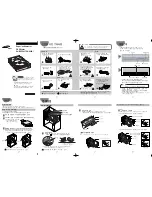
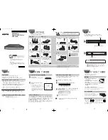
Page 18: ...2 2 Pick up A Release 1 screw C and remove the Pick up Pick up Unit Pick up C Fig 2 2 18 ...

Page 19: ... 032 452 020 021 050 430 005 035 004 006 A B C D E F G H 1 2 3 4 5 452 024 481 034 027 026 033 025 430 419 020 453 031 036 453 003 002 010 011 009 008 012 016 015 013 PBM00 MAIN C B A PBF00 FRONT C B A 482 482 482 001 482 19 20 EXPLODED VIEW ...

Page 20: ...hanged conditions of disc and change in operating temperature Jitter The 16 value of the time variation between leading and trailing edges of a specific I3 I11 pit or land as measured by Time Interval Analysis Deviation The difference between a fixed value of Pit length and Land length TOC Table Of Contents in the Lead in Area the subcode Q channel contains information about the Tracks on the disc...

Page 21: ...pitch p Radial Direction Iw A O a a Groove Land Radial Error Signal The Groove wobble Average center Actual center CD ROM READ ONLY DISC a 30nm ITEM CD ROM CD R CD RW Standard Yellow Book Orange Book II Orange Book III Record Not available Write once Re Writeable Tracking Signal I11 Itop 0 6 0 6 0 55 M11 0 70 HF Modulation Read Laser Power mW 0 5 mW 0 7 mW 1 0 mW Jitter 35 nsec 35 nsec 35 nsec Ref...

Page 22: ...t and Land on the disc It is so called WORM Write Once Read Many CD It is composed of polycarbonate layer Organic dye layer Reflective layer and Protective layer Gold Silver Reflective layer is used to enhance the reflectivity According to the kinds of Organic dye layer it is divided by Green CD Gold CD Blue CD Laser Wavelength 780 nm Laser Power read 0 7 mW Recording Power 8x 14 20mW 16x 25 35mW ...

Page 23: ... reading is enabled by the difference of reflectivity It is possible to overwrite about 1000 times Laser Wavelength 780 nm Laser Power Read 1 0mW Recording Power Erase 4 18mW Write 6 45mW When disc rewriting new data is overwritten previously recorded data Polycarbonate layer has a Pre Groove which make a track Lens H D Beam Spot Focusing Lens Laser Spot at Constant Read Intensity Reflected Light ...

Page 24: ...Spot Recorded Mark Reflected Light Signal Reflected Light Signal Below ORP Mark Too Short At Optimum Record Power ORP Above ORP Mark Too Long Time 6 Writing process of CD RW Disc Write Power Erase Power Read Power Groove Crystal Amorphous Amorphous Recorded state lower reflectivity Melting quenching Heating gradual cooling Crystal phase Erased state higher reflectivity ...

Page 25: ...Area Lead out Area Center hole Clamping and Label Area Information Area PCA PMA Test Area Count Area Diameter 15 mm Diameter 45 mm Diameter 120 mm Unrecorded Disc Tsl 00 35 65 Tsl 00 15 05 Tsl 00 13 25 Tsl 99 59 74 00 00 00 in out Test Area for performing OPC procedures Count Area to find the usable area immediately in T A Tsl start time of the Lead in Area as encoded in ATIP PMA Program Memory Ar...

Page 26: ...ad_In area so that general Driver can read it Because PCA and PMA area exist before Lead In area General CD Player or CD ROM Drive can t read these areas 9 OPC and ROPC 1 OPC Optimum Power Control This is the first step of writing process because CD writer has its own laser power value and media have different writing characteristics This is determined by the Writing characteristic speed temperatu...

Page 27: ...a close Reference B level value c Normalization of B level is used to eliminate the effect of reflectivity fluctuation The reflected B level value is normalized by the disc reflectivity itself CD R RW Media Write Strategy Determination PCA Test Area Program Area PMA Area Lead In Area Lead out Area OPC PCA Count Area ROPC Recording Capacity of CD R RW 74Minute Recording media 2048 Byte Sector X 75 ...

Page 28: ...32 The differences of DVD R RW DVD R RW discs and DVD ROM 1 Recording Layer LPP Land Pre Pit DVD R RW Disc DVD R RW Disc 0 74um 3T 0 4um DVD ROM Read Only Disc ...

Page 29: ...itch 0 74 0 74 0 74 0 74 0 74 0 74 Minimum pit length 0 4 0 44 0 4 0 4 0 4 0 4 Modulation 0 6 0 6 0 6 0 6 0 6 0 6 Channel bit rate 26 16MHz 26 16MHz 26 16MHz 26 16MHz 26 16MHz 26 16MHz Wobble Frequency 140KHz 140KHz 817 4KHz 817 4KHz Addressing 26 16MHz 26 16MHz Wobble LPP Wobble LPP Wobble ADIP Wobble ADIP Read Power mW 0 7 0 1 0 7 0 1 Write Power mW JItter 8 8 8 8 9 9 Bondinglayer Polycarbonate ...

Page 30: ...ing layer dye Disc substrate Adhesive layer Protective layer Reflective layer Dye layer Substrate Laser beam Disc structure Disc structure Recording Recording is done by changing the organic dye layer and the substrate with a laser when a strong is applied to a disc the temperature of the ortanic dye material goes up the dye is decomposed and the substrate changes at the same time At this time a d...

Page 31: ... Recording layer Phase change material Dielectric layer Disc substrate DVD RW Adhesive layer Protective layer Reflective layer Dielectric layer Recording layer Phase change material Dielectric layer Disc substrate Disc structure Recording principles Recording When a high power laser is applied to the recording material it melts and then becomes amorphous with a low reflection coefficient when it q...

Page 32: ...lses a blocked write strategy where each single mark is created by one continuous pulse 1 1st Method Using Pulsed Write Strategy 3T NRZI T 3 2Tw Ttop dTtop dTle Pb top top le Pp Channel bits N 3 only the top pulse T first pulse lead time dT dT NRZI T 4 2Tw Tw Ttop Tmp Tmp Tlp dTtop dTle Pb top top le lp mp Pp Channel bits N 4 the top pulse T multi pulse T and last pulse T first pulse lead time dT ...

Page 33: ...Tw 1 25Tw dTtop 4 dPp4 Ttop 4 Tlp Ttop 4 Ttop 4 Tmp Tmp Tlp Tlp Tmp N 3 T cm 3 can be optimized individually N 4 T cm 4 x N 3 T T T T P shall be 0 1mW top mp lp w w top c Pp Actual write power Pb Bias Power dPp Additional power Only be applied for the 3T and 4T marks Pc Cooling power Especially at higher recording speeds optimum cooling down of the recording layer after writing a mark may be neede...

Page 34: ...38 5 Writing Pulse Wave Form of DVD RW NRZI Channel bits 2Tw Tw Ttop dTtop Pp Pe Tmp mp T dTera Pp Actual write power Pe Erase Power Pb Bias Power Pb 0mW Tmp ...

Page 35: ...corded Disc PSN 23080H 27080H 27480H 28480H 2A480H 30000H 260540H 261940H 262940H 263940H 267940H in OUT Disc Center Rim area Center hole 1st transition area 2nd transition area Clamping Zone 3rd transtion area Information Zone Diameter 15 mm Diameter 16 mm Diameter 22 mm Diameter 33 mm Diameter 44 mm Diameter 120 mm Disc Center Rim area Inner Disc Count Zone Outer Disc Count Zone 2 Layout of DVD ...

Page 36: ...f OPC algorithm performed in IDT Zone Lead in Zone Lead out Zone Data Zone Inner Disc Test Zone Outer Disc Test Zone Unrecorded Disc PSN 2A480H 2A7C80H 2DC80H 30000H 260540H 262940H 265940H 266140H in OUT Center hole 1st transition area 2nd transition area Clamping Zone 3rd transtion area Information Zone Diameter 15 mm Diameter 16 mm Diameter 22 mm Diameter 33 mm Diameter 44 mm Diameter 120 mm Di...

Page 37: ...e Media 1 LightScribe Media Center Hole Screen Printed Imaging Layer Clear Protective Coating Reflective Thermal Layer Dye Data Layer Polycarbonate Substrate DiscOD Label Zone Control Feature Zone Clamping Logo Zone ...

Page 38: ...nalog Signal Processor MECHANISM Optical Pick up Optical Encoder Sled Track Tilt Focus RFOUT Spindle Motor Step Motor Track Actuator Tilt Actuator Focus Actuator Laser Power Reference Write Strategy Control Buffer Memory SERVO Signals RF Cell Signals Laser Power Monitor Signal Optical FG CIrcuit ...

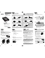
Page 39: ...43 3 MD Assy For LightScribe Optical Encoder Unit OPU ID Movement Range L 21um ...

Page 40: ...L OR CODESTRIP FFC 3PIN SIGNAL PROCESSING CIRCUITRY R VLED VCC CH A CH B CH B GND GND Vcc OFG Encoder PCB PIN 6 VCC PIN 5 CH A PIN 4 GND PIN 3 VLED PIN 2 GND PIN 1 CH B PIN 6 VCC PIN 5 CH A PIN 4 GND PIN 3 VLED PIN 2 GND PIN 1 CH B Optical Encoder IC Schematic of Enc PCB ...

Page 41: ...lice EFM demodulator CiRC error correction Audio DAC Buffer Memory controller CSS controller Atapi interface control Data PLL Servo ADC Focus tracking control output Sled control output CAV Spindle control P up Unit LPC 812R IC121 RF AMP AN22113A CD DVD IC201 MN103SA6G TE CSO GEN FE GEN IC261 DRAM IC262 Flash ROM SRAM ...

Page 42: ... the regional code and plays title in the case of allowed regional code only 2 Management of DVD Disc for the scrambled of data 1 DVD ROM and DVD player of host generate the KEY 1 respectively transfer to opposite part the KEY 2 is received recognizes the data transfer or not with this value and generates the bus key encoded the data 2 Encoded Disc Key and Title Key host is transfer with the bus K...

Page 43: ...MPEG 2 board generates the challenge key 10 Byte and transfers to drive The board and drive generate key 1 5Byte with the challenge key respectively Of course the Algorithm generating the key 1 is not known 3 Compare with the generated key 1 if it corresponds each other the first step of authentication is completed This is a course to identify the MPEG 2 board with a drive 4 The second step of aut...

Page 44: ...UM PLW PNG NZL AUS 4 The disc has the regional code of 8 bit Example The disc manufactured in the U S A has the number one Transfer to MPEG 2 board reading the regional code Receiving data from the MPEG 2 board and output through the monitor If the board is setting to the regional code 1 for the U S A Check the received regional code to number 1 all or not transfer the data to VGA card in accordan...

Page 45: ...9 EF3 10 C 11 D 12 SW PDIC 13 RF 14 RF 15 SW FM 16 VCC FM 17 GND FM 18 VREF FM 19 FM_OUT 20 TEMP 21 GND Themester 22 W1DISN 23 W1DIS 24 W2DISN 25 W2DIS 26 W3DISN 27 W3DIS 28 OSCEN 29 GND 30 GND 31 VCC 32 W3SET 33 W2SET 34 W1SET 35 RSET 36 OUTSET 37 ENABLE 38 VCC 39 GND 40 F Focus Actuator TILT TRACK 41 F 42 TILT 43 TILT 44 T 45 T 9 10 11 12 13 14 6 5 4 3 2 1 10 1 2 3 4 5 9 8 7 6 13 6 NE2 5 E2 4 ER...

Page 46: ...DISN LVDS control for output current Low Enable 25 W2DIS LVDS control for output current High Enable 24 W2DISN LVDS control for output current Low Enable 23 W1DIS LVDS control for output current High Enable 22 W1DISN LVDS control for output current Low Enable 21 GND FPD Ground connection for PDIC FPD TEMP 20 TEMP Output voltage for controlling temperature 19 FPD OUT APC amplifier output 18 VREF FP...

Page 47: ...d A D B C k x EF1 EF4 EF2 EF3 This signal is generated in RF IC IC121 AN22113A and controls the pick up s left and right shift to find to track on Disc 3 RF Signal A B C D This signal is converted to DATA signal in DSP IC IC201 MN103SA6G 51 Pick Up module Photo Diode Tracking Focusing Infrared Iaser k F H E G A D B C A D B C k F H E G Offset TE Tp Sub2 Main Tp 2 Sub1 Track Center F E D C A B H G ...

Page 48: ...Circuit Operation The ALPC block detects the laser output power of the front monitor The power signal detected with the PD for front monitor detection is input the voltage from the VPD pin 123Pin or the FPDM pin 127Pin the reference signal of the input signal is input from the VREFPD pin 124Pin The ALPC block generates the singals from the input laser power signals in the following detection syste...

Page 49: ...A B C D E F G H A B C D E F G H IC121 A N22113A FE TE IC201 Servo Control MN103SA6G TE FE A D D A C SLED COMPENSATOR A D PARALLEL DIGITAL COMPENSATOR SDRV 60 64 66 67 STEP2 STEP1 IC301 BD7956FS 29 30 M Stepping Motor Logic A 37 38 40 39 A B B Tracking Focusing Actuator T T F F 5 4 LEVEL SHIFT FDRV TDRV LEVEL SHIFT 53 54 51 52 Focus Tracking Sled Servo ...

Page 50: ... S DPWM 10bit 100 50 MHz S DPWM 10bit 100 50 MHz ADC INT LPF V ref R On Off BD7956 Drive IC AN22113 FEP MUX Circuit R On Off 16 bit Timer RXD RFS_iNT HC_CTL RXD RFOUT Track Focus Internal u P F W Need to change to 16bit MN103SA6G MECHANISM Comparator RFOUT RXD RFS_INT ...

Page 51: ...e servo is as following 1 Wobble CLV 4x 10x 16x 24x 32x 40x Blank area in CD R CD RW 2 Wobble CLV 1x 2x 2 4x 4x 8x Blank area in DVD R RW 3 CD 15x CAV Video CD CD DA Audio out 4 CD 32x CAV CD RW CD DA DAE 5 CD 40x CAV CD ROM R 6 DVD 8x CAV Single Layer DVD ROM Movie Dual Layer DVD ROM DVD RW DVD RW DVD R Double Layer 7 DVD 10x CAV DVD R DVD R 6 DVD 16x CAV Single layer DVD ROM Data Spindle Servo i...

Page 52: ...g the LightScribe 56 MN103SA6G MECHANISM BSDA 12bit 100MHz Internal u P F W 16bit Timer Pre scale FEP INT X TAL 16 9344MHz TR Optical Encoder IC 5V Optical FG 69 9 2 or 3 state R On Off BD7956 Drive IC Motor Optical Encoder Enc Vcc ...

Page 53: ... COFTR 15 VCC6 16 VHALF 17 CTC 18 CXDPH1 19 CXDPH2 20 MOUT2 25 GND1 26 PO0 27 PO1 28 PO2 29 PO3 30 PO4 31 PO5 32 PO6 33 STMOUT 39 TC 40 OFTR 41 BDO 42 VCC51 43 GND5 44 WTGT 45 PIO0 34 PIO1 35 PIO2 36 PIO3 37 FEPIDGT SH6 46 NC 47 WIDGT SH4 48 SH3 49 SH2 50 SH1 51 SH5 52 VCC4 53 SEN 54 SCK 55 SDAT 56 RSEN 57 RSDAT 58 VCC52 59 GND4 60 ASENV LPPM 61 LPPS 62 WBL 63 CLUMPGT 64 PAD0 65 PAD1 66 PAD2 67 PA...

Page 54: ...SFEPN SMTEP SMTEN SSTEP SSTEN SDAAOUT SDABOUT SDACOUT SDADOUT SDPDTEP SRFMA SRFMD SRFMB SRFMC SDPDTEN SPLAOUT SPLBOUT SPOF TCOP TCO TCON TIOP TIO SBDOAS TION VGA VGA COMP PK ENV PK ENV COMP VGA Bypass VGA Bypass M P X M P X DPD TE Dtetction TC TI Dtetction HDVREF VHALF VREF08 RFP CDRFP RFN CDRFN BDO RF OUT RFIN1 RFIN2 EQOUTP EQOUTN VREF GATE All Sum VG A Group delay compensation SW To Each Block P...

Page 55: ...ply pin for DPD internal current source power supply pin 3 3V 17 VHALF O 1 2 VCC 3 3V output pin 18 CTC I Capacitor connection pin for TE binary floating 19 CXDPH1 I PH capacitor connection pin 1 for LPOS 20 CXDPH2 I PH capacitor connection pin 2 for LPOS 21 SEO1 O Output pin 1 after selection of each error signal 22 SEO2 O Output pin 2 after selection of each error signal 23 MOUT0 I Analog monito...

Page 56: ...in pulldown 52 SH5 I Sample and hold timing signal input pin of wobble S H at recording pull down 53 VCC4 PS Power supply pin for internal LOGIC 5 0V 54 SEN I Serial enable input pulldown 55 SCK I Serial clock input pullup 56 SDAT I O Serial signal data input 57 RSEN I Serial enable input for RF pulldown 58 RSDAT I Serial signal data input for RF 59 VCC52 PS Power supply pin for CMOS I F internal ...

Page 57: ...92 CWAGC1 I AGC adjustment capacitor connection pin 1 for WBL extraction 93 CWBLHPF2 I Capacitor connection pin for N side HPF before WBLAGC 94 CWBLHPF1 I Capacitor connection pin for P side HPF before WBLAGC 95 RFP I DVD RF differential input pin 96 RFN I DVD RF differential input pin 97 CDRFP I CD RF differential input pin 98 CDRFN I CD RF differential input pin 99 CDHPF I Internal RF additional...

Page 58: ... pin 1 121 FIN I CD sub signll input pin 2 122 N C 123 N C 124 DACOUT O Wide Use DAC output pin 125 VREF08 O 0 8V referece Voltage output for APC pin 126 VPD I DVD front monitor signal input pin for APC 127 N C I 128 VREFPD I Front light system reference level input pin I Input pin O Output pin I O I O pin PS Power supply Ground pin N C Non Connection ...

Page 59: ...RC CDA1 AVSSDRC P02 FMSW PO3 WTGT WBL FEPIDGT SH5 WIDGT SH3 SH2 SH1 TC CLUMPGT ASENV POLGT LPPS OFTR P04 GENE0 TRCDATA3 EXTRIG2 TGCHG P05 LSEN FADR3 FADR2 FADR1 MA4 MA3 MA5 MA2 MA6 MA1 MA7 MA0 VDD3 VSS MA8 MA10 MA9 P15 TRCDATA3 EXTR1G2 MBA1 P14 TRCDATA2 EXTR1G1 MA11 MBA0 MCKB MNRAS MCLK MNCAS MDQMU MNWE MDQML VDD3 VDD12 VSS MDQ8 MDQ7 MDQ9 MDQ6 MDQ10 MDQ5 MDQ11 MDQ4 MDQ12 MDQ3 MDQ13 MDQ2 MDQ14 MDQ1...

Page 60: ... Block Diagram SODC MN103SA6G 64 FEP LDD FEP DRC CD SERVO ADSC CD REC PERIPHERAL 32 bit CPU ANALOG CPU BCU FMT HOST 16 9MHz SDRAM 16 Mbit 64 Mbit Falsh ROM 2 Mbyte ECC HOST I F ...

Page 61: ...ap Res Filter connection pin for wobble PLL 18 CPOP3 I O Cap Res Filter connection pin for wobble PLL 19 CPOP2 I O Cap Res Filter connection pin for wobble PLL 20 CPOP1 I O Cap Res Filter connection pin for wobble PLL 21 AVSSD1 GND GND WOBBLE analog Vpp 22 SEO1 I FEP Error signal output after selection analog input 23 SEO2 I FEP Error signla output after selection analog input 24 AVSSA GND GND Ser...

Page 62: ...GT O FEP RF AGC bias circuit clamp signal 48 ASENV I FEP ASENV LPP mark input 49 POLGT O FEP CAPA polarity switch signal sub beam sampling signal 50 LPPS I FEP LPP space input 51 OFTR I FEP Off track input 52 PO4 CPU external interrupt general purpose I O GENE0 I O Inner limit switch input TRCDATA3 Trace data 3 EXTRIG2 Trigger 2 53 TGCHG I O OEIC Write power switch signal P05 General purpose I O 5...

Page 63: ...indle FG input 5V input 72 SEN O FEP FEP serial interface enable 73 SCK O FEP FEP serial interface clock 74 SDAT I O FEP FEP serial interface data 75 RSEN O FEP FEP serial interface enable2 RF 76 RSDAT O FEP FEP serial interface data2 RF 77 BDO I FEP Dropout signal 78 MASTER I O HOST ATAPI master slave signal P23 General purpose I O 79 NRESET I HOST ATAPI reset signal 80 HDD7 I O HOST ATAPI data I...

Page 64: ...stic signal from ATAPI slave to master 110 DA0 I O HOST ATAPI host address signal 111 DA2 I O HOST ATAPI host address signal 112 NCS1FX I HOST ATAPI host chip select signal 113 VSS GND GND Digital Vss 114 VDD5 Power supply Power supply 5V reference power supply 115 VDD3 Power supply Power supply I O pad VDD 3 3V 116 NCS3FX I HOST ATAPI host chip select signal 117 NDASP I O HOST ATAPI drive active ...

Page 65: ...AM Debugging trace data EXTRIG1 Trigger MA11 SDRAM address P15 General purpose I O 146 TRCDATA3 I O SDRAM Debugging trace data EXTRIG2 Trigger MBA1 SDRAM bank switch 1 147 MA9 O SDRAM SDRAM address 148 MA10 O SDRAM SDRAM address 149 MA8 O SDRAm SDRAM address 150 VSS GND GND Digital Vss 151 VDD3 Power supply Power supply I O pad VDD 3 3V 152 MA0 O SDRAM SDRAM address 153 MA7 O SDRAM SDRAM address 1...

Page 66: ...LASH Flash ROM address 179 FADR13 I O FLASH Flash ROM address 180 FADR14 I O FLASH Flash ROM address 181 FADR15 I O FLASH Flash ROM address 182 FADR16 I O FLASH Flash ROM address 183 FDT15 I O FLASH Flash ROM data 184 FDT7 I O FLASH Flash ROM data 185 FDT14 I O FLASH Flash ROM data 186 FDT6 I O FLASH Flash ROM data 187 FDT13 I O FLASH Flash ROM data 188 FDT5 I O FLASH Flash ROM data 189 FDT12 I O ...

Page 67: ... data DRC monitor 0 206 SCLOCK I O Debugger clock DRC monitor 1 207 DASPST I O DASP setting TRCDATA0 Trace data 0 208 MSTPOL I O MASTER pin polarity switch TRCDATA1 Trace data 1 209 VSS GND GND Digital Vss 210 OSCI I Xtal Oscilator input 16 9344MHz 211 OSCO O Xtal Oscilator output 212 VDD3 Power supply Power supply I O pad VDD 3 3V P17 General purpose I O 213 TRCDATA2 I O Trace data 2 EXTRIG1 Exte...

Page 68: ...G FG fin fin OSC 50k 47k 33 6k 33 6k 1 54 LDO ACO1 53 ACO1 52 ACO2 51 ACO2 50 ACO3 49 ACO3 48 AV 47 ACTIN3 46 LDIN 45 AGND 44 SPCNF 43 FG 42 V 41 fin 40 SLO1 39 SLO1 38 SLO2 37 SLO2 36 SLGND 35 CTL2 34 CTL1 33 SLRNF2 32 SLRNF1 31 SLVDD C M 30 SLIN2 29 SLIN1 28 DVcc 2 LDO 3 Vcc 4 ACTIN1 5 ACTIN2 6 TJMON 7 BTHC 8 SPVM_S 9 PGND1 10 PGND2 11 U 12 SPV 1 13 V M M 14 fin 15 PGND3 16 W 17 SPV 2 18 SPRNF 1...

Page 69: ...ive input 26 SPIN Spindle driver input 27 DGND PWM block pre ground No Symbol Description 54 ACO1 Actuator driver 1 positive output 53 ACO1 Actuator driver 1 negative output 52 ACO2 Actuator driver 2 positive output 51 ACO2 Actuator driver 2 negative output 50 ACO3 Actuator driver 3 positive output 49 ACO3 Actuator driver 3 negative output 48 AVM Actuator driver block power supply 47 ACTIN3 Actuat...

Page 70: ...ction input Hall bias FG signal output 12 10 9 15 17 16 13 11 22 20 28 28 28 28 28 24 23 21 25 32 33 38 40 27 36 37 39 49 51 53 48 48 48 50 52 54 45 2 3 3 3 45 1 19 28 43 28 5 4 46 47 3 3 50k 5pF 5k 10pP Ω Ω Reference voltage input BTHC terminal TJ output 29 30 28 28 47k 3pF Ω 3 40kΩ 100 113 Ω Ω 5kΩ 26 28 28 47k 5pF Ω 5k Ω Control signal input 34 35 28 28 50kΩ 50kΩ 50kΩ 1 1 1 20 6 18 8 8 2kΩ 12 5k...

Page 71: ...IC Check the IC201 IC121 Does the pin 1 Reset of IC271 change 0V to 3 3V at the power supply initial input mode Power Is the pin 5 of IC401 3 3V Reference 1 65V VREF Check pin113 of IC121 2 2V HDVREF Check pin78 of IC121 NO NO YES YES YES YES 75 Are the X201 oscillating Check the X201 16 9MHz Check the IC201 NO Check the IC401 NO Check the IC121 NO Check it after connecting the power cable only on...

Page 72: ...e tray Insert DVD R RW Disc and check rotation Does Disc rotate continuously and the drive recognize the disc Does Disc rotate continuously and the drive recognize the disc Does Disc rotate continuously and the drive recognize the disc Go to Sled operating is abnormal Go to Laser operating is abnormal Go to Recognition fail Case1 CD ROM Disc Go to Recognition fail Case2 Blank CD R RW Go to Recogni...

Page 73: ...connction of IC201 pin 203 Replace the EJECT SW Check the connctor CN303 Replace the IC301 Is the input voltage 0V at IC201 pin204 OPENSW when push the SW1 Is the input voltage 0V at IC201 pin63 LOADSW when push the SW1 YES NO NO Check the connction of IC201 pin 66 Replace theIC201 Check the communication line between IC201 NO YES YES YES NO Is there Tray drive voltage output IC301 pin 1 2 Is ther...

Page 74: ...1 Is DRVMUTE2 signal H IC301 pin 35 Check the R316 R317 Check the connection of IC121 pin 32 Is there Sled drive voltage output CN302 pin 1 2 3 4 Replace the Sled Motor YES NO NO YES YES Check the Connection CN302 NO Is there Sled drive voltage input IC301 pin 29 30 YES NO Is there Sled drive voltage output IC301 pin37 38 39 40 YES NO ...

Page 75: ...oltage output IC301 pin 11 13 16 Is there Spindle drive voltage output IC301 pin 1 2 3 Check the Connection CN301 Replace the Spindle Motor NO NO NO YES YES Is there FG signal input IC201 pin 71 NO YES YES Check the output of IC301 pin 43 Check the connector CN301 Replace the IC301 Replace the IC201 OK ...

Page 76: ...rmal Is there Focus Search control signal input IC301 pin5 Is DRVMUTE2 signal H IC301 pin 35 ReplacetheIC301 ChecktheconnectionCN101pin40 41 Check the connection of IC121 pin 32 Replace the IC121 NO YES Replace the Pick Up Is there Focus Search drive voltage output IC301pin51 52 NO Check the connection of IC201 pin 62 Check the communication line between IC121 and IC201 Replace the IC201 YES NO YE...

Page 77: ...121 NO Replace the IC201 Check the Drive IC IC301 and P U referring to Focus Actuator operating is abnormal Is there TDRV signal output in Tracking ON IC201 pin66 NO Is PICK UP E F G H output normal CN101 pin 8 5 9 4 YES YES NO IC121 pin24 is MOUT1 FEP Monitor1 After disc recognition action Monitor port is off So please check TE signal during disc recognition ...

Page 78: ...p RF signal IC121 Pin81 RFOUT was 2 2 5V NO Go to LD CHECK YES NO ReplaceIC121 YES Check EQOUTP waveform IC121 Pin 74 was 1 75 2 3V NO Goto TrackingServoisunstable YES YES Check after replacing IC201 It is OK NO Recognition Fail Case2 Blank CD R RW Is there WBL IC201 pin39 signal Check the connection between IC201 and IC121 Replace IC121 Replace the IC201 NO YES Is there WBL IC121 pin63 signal NO ...

Page 79: ...il Case 4 Blank DVD R RW Replace IC201 Replace IC121 Check the connection between IC121 and IC201 YES NO NO Is there WBL IC201 pin39 Signal YES NO Is there RF signal at IC121 Pin81 YES Replace the Pickup NO Replace the IC121 Is there RF signal at IC121 Pin95 RFP and Pin96 RFN YES NO Replace the IC201 Check again after the replace IC121 It is OK OK ...

Page 80: ...o Writing Part Check YES NO Remove the Dust Fingerprint and if the disc has long width Scratch change it Does the disc have any Dust Scratch Fingerprint YES NO Use LG bundle Software Write Tool Version Is the write Tool version supported by LG DVD RW Drive YES NO NO Check disc information on Writng Tool If you get some data information with Non Recordable Disc Message the disc is finalized Finaliz...

Page 81: ...C121 Audio Play AUDMUTE H Check and replace the IC201 Check the connection of L R OUT Insert the audio Disc NO AUDMUTE L IC121 Pin 33 DSP ROUT LOUT signals output IC201 Pin 10 11 Do audio Line signals output CN271 pin 51 54 NO NO YES YES Normal ...

Page 82: ...nness of Media Check 3pin FFC and Q501 Check Encoder IC Power NO YES Check Enc Assy s Alignment and Grease on it Check the OFG Signal NO YES Go to LD CHECK Check P U Read Power 4 5 5 5mW NO YES Replace IC501 502 Check the RXD RFS_INT Signal On Recognizing LS Media NO YES OK ...

Page 83: ...same Directory 3 If you use GWA 4164B Dragon 2005 04 08 14 00 will be displayed on the window Frame 4 Select I F Setup on the menu bar 5 Select ATAPI I F and then Click OK 6 Select Target Device on the menu bar 7 Select DVDRRW GWA 4164B on Target Device and then Click OK How to use Test Tool Dragon I F Setup Menu Target Device window ...

Page 84: ...Para tab and verify the specification ALPC Parameters 1 CD VRDC 117 153 2 CD VWDC_NMP 100 135 3 CD VWDC_MP 100 137 4 CD VWDC_ERASE 105 135 5 DVD VRDC 115 157 6 DVD VWDC_NMP 100 135 7 DVD VWDC_MP 100 135 8 DVD VWDC_ERASE 105 140 9 H C VWDC 100 150 10 Default ALPC Para used 0xFF 4 Close window ALPC Parameters Menu Additional Function Menu ...

Page 85: ...P Power box ex 16 45mW 1645 12 08mW 1208 7 Click MP button and measure LD Power with Power meter Type the result in the blank RW Erase Power box 8 Click ERASE button and measure LD Power with Power meter Type the result in the blank RW Erase Power box 9 Click LD Off button and then click Setup button and result witll be displayed with OK or NG 10 Select HC_CD and then click HC button 11 Measure LD...

Page 86: ...90 CD Laser Power Setup Result HC_CD Laser Power Setup Result DVD Laser Power Setup Result ...

Page 87: ...C201 MN103SA6G Pick up LPC 812R BA3259 IC401 3 3 1 2V Reg 5V_source Reset IC IC271 BD5233 Drive IC Actuator BD7956 RF IC IC121 AN22113A DSP IC IC201 MN103SA6G Pick up LPC 812R AT22138A IC101 SDRAM IC261 M12L16161A Flash Memory IC262 EEPROM IC201 MN103SA6G MX29LV160BBTC Power Supply System Diagram ...

Page 88: ... RF EQ GCC Wobble JLINE MPX Write Strategy LVDS Serial I F ADC Servo ADSC FMT Servo DRC ECC BCU 1M bit DRAM 32bit CPU Host I F Host PC Authoring Tool Buffer RAM PWM BSDA Controller Serial I F FEP RF AN22113A SODC DSP MN103SA6G I V AMP Spindle motor Spindle Driver 92 BLOCK DIAGRAM ...

Page 89: ... Block BDO Block RFEQ Block JLINE Block LOGIC Block RF Gene Block GATE Block To each Block VREF Block TEC Block LPOS Block SDRAM 16 64Mb Built in System Controller 32Bit CPU Flash ROM AD ADIP DRC CD ADIP FORMATTER ECG EEPROM 4KByte AD SRAM ADSC DA VCO CIRC CD PRE ANALOG SERVO DSP 32bit CD REC PERIPHERAL BCU A D AUTH SYSIF INTC TMR KCGEN MODEC WDT AM DMA ENC DEC HOST I F ATAPI I F MPEG I F RV7 MN10...

Reviews: