background image

- 8 -

OPERATING INSTRUCTIONS

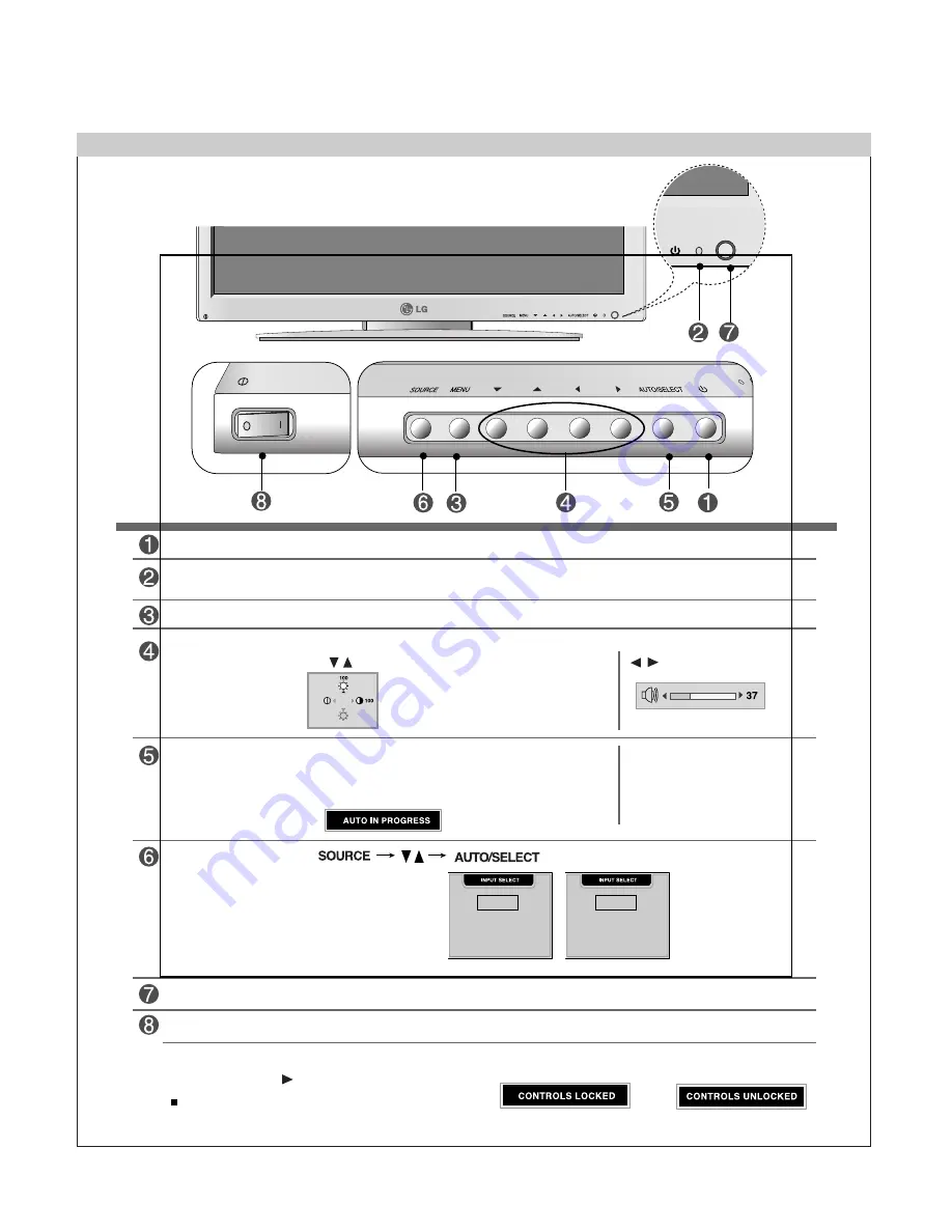
Front Control Panel 

•  Press the button to turn on the power. Press the button again to turn it off.

•  This Indicator lights up green when the display operates normally. If the display is in DPM

(Energy Saving) mode, this indicator color changes to amber.

Power Button

Power LED

• Adjust the volume.

• Use this button to directly control

brightness and contrast of the PC signal
(DSUB/DVI).

•  Use this button to show/hide the OSD (On Screen Display) menu screen.

MENU Button

• Use the button to select an icon or adjust the setting in the OSD screen.

OSD Select
Adjust Button

[A] For DSUB signal
• Select the icon to adjust on the OSD screen.
• If you press the [AUTO/SELECT] button, automatic

screen adjustment will be started.

[B] Other signals that DSUB
• The current signal and mode

information will be displayed.

AUTO/SELECT Button

• The unit that receives the signal from the remote controller.

DVI DIGITAL

DVI digital signal

DSUB ANALOG

15-pin D-Sub analog signal

VIDEO1(CVBS)

Composite video

VIDEO2(S-Video)

S-Video

SCART 1/ 2

Composite

COMPONENT 1/ 2

YPbPr (YCbCr)

• Select the input signal 

SOURCE Button

[Case 1]

DVI DIGITAL

DSUB ANALOG

VIDEO1(CVBS)

VIDEO2(S-Video)

SCART 1

SCART 2

[Case 2]

DVI DIGITAL

DSUB ANALOG

VIDEO1(CVBS)

VIDEO2(S-Video)

COMPONENT 1

COMPONENT 2

• OSD is locked 

• OSD is unlocked.

Use this button to lock/unlock OSD screen adjustment.

(Activated when pressed together longer than 5 seconds.)

OSD Lock/Unlock Button

Menu button  + 

• Use this button to turn on/off the monitor.

Main Power Switch

http://www.wjel.net

Summary of Contents for Flatron L4200A

Page 1: ...ttp www LGEservice com techsup html CAUTION BEFORE SERVICING THE UNIT READ THE SAFETY PRECAUTIONS IN THIS MANUAL CHASSIS NO CL 49 MODEL L4200A L4200AL AL A L4200A L4200AFL AL A L4200A L4200APL AL A L4200A L4200ATL AL A Same model for Service h t t p w w w w j e l n e t ...

Page 2: ...h t t p w w w w j e l n e t ...

Page 3: ... Video Cross Talk 43 3 5 Sync Input Horizontal 30 83kHz Digital 30 72kHz Vertical 56 85Hz Input Form Separate TTL Positive Negative Digital 4 POWER SUPPLY 4 1 Power Voltage AC 100 240V 50 60Hz 4 2 Power Consumption 5 ENVIRONMENT 5 1 Operating Temperature 10 C 35 C 50 F 95 F 5 2 Operating Humidity 10 80 5 3 MTBF 50 000 Hours Min 6 DIMENSIONS with TILT SWIVEL L4200AL L4200ATL Width 1057 mm 41 61 Hei...

Page 4: ...1 T M D S Data1 T M D S Data1 3 Shield T M D S Data3 T M D S Data3 5V Power Ground return for 5V H Sync and V Sync Pin Signal DVI D 1 8 9 17 24 16 16 17 18 19 20 21 22 23 24 Hot Plug Detect T M D S Data0 T M D S Data0 T M D S Data0 5 Shield T M D S Data5 T M D S Data5 T M D S Clock Shield T M D S Clock T M D S Clock T M D S Transition Minimized Differential Signaling DVI D Connector Digital h t t ...

Page 5: ...l or pen as this may result in damage to the panel Protect the module from the ESD as it may damage the electronic circuit C MOS Make certain that treatment person s body are grounded through wrist band Do not leave the module in high temperature and in areas of high humidity for a long time The module not be exposed to the direct sunlight Avoid contact with water as it may a short circuit within ...

Page 6: ...9 94 525 480 10 2 33 4 H 31 5 37 5 840 640 16 64 120 640 x 480 V 75 500 480 1 3 16 5 H 36 0 43 269 832 640 56 56 80 640 x 480 V 85 0 509 480 1 3 25 6 H 40 0 37 879 1056 800 40 128 88 800 x 600 V 60 317 628 600 1 4 23 7 H 49 5 46 875 1056 800 16 80 160 800 x 600 V 75 0 625 600 1 3 21 8 H 56 25 53 674 1048 800 32 64 152 800 x 600 V 85 061 631 600 1 3 27 9 H 57 283 49 725 1152 832 32 64 224 832 x 624...

Page 7: ...0 x 1200 V 60 1250 1200 1 3 46 Mode H V Sort Sync Porarity DOT Clock Frequency Total Period E Video Active Time A Front Porch C Sync Duration D Back Porch F Resolution 1 H 25 175 31 469 800 640 16 96 48 SDTV V 59 94 525 480 10 2 33 480P 2 H 27 027 31 5 858 720 16 62 60 HDTV V 60 525 480 10 2 33 720P 3 H 74 176 44 955 1650 1280 70 40 260 HDTV V 59 94 750 720 5 5 60 720P 4 H 74 250 33 750 2200 1920 ...

Page 8: ...of the PC sound card is checked before connecting If the Audio Out of PC sound card has only Speaker Out reduce the PC volume If the Audio Out of the PC sound card supports both Speaker Out and Line Out convert to Line Out using the card jumper of the program Refer to the Sound Card Manual Case 1 Case 2 RS 232C Serial ports PC signal inputs Connect the audio cable to the LINE OUT jack of the PC so...

Page 9: ... SELECT button automatic screen adjustment will be started B Other signals that DSUB The current signal and mode information will be displayed AUTO SELECT Button The unit that receives the signal from the remote controller DVI DIGITAL DVI digital signal DSUB ANALOG 15 pin D Sub analog signal VIDEO1 CVBS Composite video VIDEO2 S Video S Video SCART 1 2 Composite COMPONENT 1 2 YPbPr YCbCr Select the...

Page 10: ... not a function which is supported Menu Button Exit Button Auto Button PC Automatic adjustment function Operational for the analog signal only Check Button Sound Mode Select Select the sound mode MONO STEREO Video Operation Button Applicable for LG products only Volume Button Mute button There is not a function which is supported PSM Button When watching AV DVD HDTV Automatically adjusts the image...

Page 11: ...se 1 CVBS S Video SCART1 SCART 2 Case 2 CVBS S Video COMPONENT1 COMPONENT2 DVI DIGITAL DSUB ANALOG VIDEO1 CVBS VIDEO2 S Video SCART 1 SCART 2 Case 2 DVI DIGITAL DSUB ANALOG VIDEO1 CVBS VIDEO2 S Video COMPONENT 1 COMPONENT 2 1 PIP Picture in Picture Button The sub screen moves to the next mode whenever you press this button SMALL LARGE OFF 2 POP Picture out Picture Button The sub screen moves to th...

Page 12: ...en displays Input Signal 2 the sub screen can display Input Signal 1 only You can swap Input Signal 1 and Input Signal 2 using the SWAP button CVBS CVBS S Video S Video SCART 1 COMPONENT 1 SCART 1 COMPONENT 1 SCART 2 COMPONENT 2 SCART 2 COMPONENT 2 3 Swap Button You can swap the main screen and the sub screen when the PIP POP PBP function is used PIP POP PBP h t t p w w w w j e l n e t ...

Page 13: ...N 6631T25019E 5PIN 6631T20029S 13PIN 6631T20029U 14PIN 6631T20029R 5PIN 6631T25019D Power Cord Switch Screw 11Pin 13Pin 5Pin 15Pin 14Pin 14Pin 14Pin 14Pin 15Pin 15Pin 15Pin 5Pin 5Pin 10Pin 10Pin 6Pin 6Pin 8Pin 8Pin 8Pin 8Pin 20Pin 20Pin 5Pin 5Pin 5Pin 13Pin 12Pin 12Pin 12Pin 12Pin 12Pin 12Pin Inverter Inverter Power Board Main Board 2Pin 3Pin 4Pin 2Pin 1Pin 11Pin Screw Screw Screw 1 8 9 10 11 12 1...

Page 14: ...D 2 5V_3D 3DY C I2C EN_3D RST_3D CSI_3D CVBSO_SC SCART_Select S_AVID 1 S_AVID 2 S_AVID R G B_In1 FB_In T_R G B T_FB S_R G B S_FB 5V_BA RGB_Select I2C 3 3V_TXT 2 5V_TXT SW_Tuner 0 1 Buffer Vout_TXT 5V_VPC SCL1 SDA1 3 3V_M Data 0 10 Address 0 31 1 8V_FIL 3 3V_FIL 13 5MHz CLK_ADC HS_ADC VS_ADC 3 3V_F FDATA 0 7 FADDR_ 0 18 WE_F RE_F CS_F DDRDATA 0 31 DDRADDR_ 0 11 2 5V_DDR 3 3V_M 2 5V_M 1 8V_M DVI _RX...

Page 15: ..._VPC B F E G CVBS_In S_CV1 S_CV2 H BA 7657F 5V_BA RGB_Select R G B Out_FIL R G B In_ANA R G B In SOG SCL2 SDA2 SCL2 SDA2 D Sub EEPROM 24C16 I2C_DDCCI 3 3_ADC SCL1 SDA1 SY SC_In Y C1 Y C2 CVIN1 CVIN2 CVIN3 CVIN4 CVIN5 Y C OUT CVOU T1 CVOU T2 CVOU T3 CXA2040Q CVBSI_3D 9V_CXA Y Cout_CXA C D S_R G B S_FB I Port 1 Port A J Port 2 NTSC Option Compo_In Compo_In YPbPr_In RS232C MST9888 BA 7657F YPbPr_In h...

Page 16: ...Out SIF1 CVBS Audio_In Audio Buffer To Speaker Out DACM_L DACM_R AMP IN_R AMP IN_L SCART_In_Out Half SC1_In SC2_In SC3_In SC4_In SCART Audio2_Out SC2_OUT 8VA PC Audio_Select PC Audio_Sta ndby 8VA 5VS MSP_INT I2C_SCL I2C_SDA MSP_RST Tuner SIF MONO_In SECAM_Audio 8VA 8VA 18VAMP Standby_TPA3004 Fadeout_Audio RS232_In RS232_Out MAX232 Tx Tx_In Tx_Out Rx Rx_In Rx_Out Option Board ł ł ł ł º º º º CVBS_O...

Page 17: ...6 6 6 6 0 0 0 0 H H H H z z z z INPUT RECTIFIER AND FILTER MAIN SWITCHING TRANSFORMER OUTPUT RECTIFIER AND FILTER MAIN CONTROL IC CIRCUIT INVERTER SWITCHING TRANSFORMER INVERTER CONTROL IC CIRCUIT PFC CHOKE COIL PFC CONTROL IC CIRCUIT OUTPUT RECTIFIER AND FILTER F B F B F B 400V Vcc 5V Stand by 12V 18V 12V or 24V MICOM PWR O n Off Vcc L N h t t p w w w w j e l n e t ...

Page 18: ...the audio amplifier is that to amplify audio L R signal transmitted from audio decoder The audio signal is amplified according to pre defined DC volume control curve Also Headphone amplifier Tpa6110 U501 is controlled through Line out 6 De interlacer This block is composed of FLI 2310 U301 and peripheral devices GM1501 U402 controls this IC through IIC Line And this IC converts 8 Bit Interlaced Y ...

Page 19: ...to LCD Monitor only 1 Port Setup a Copy UserPort sys file to c WINNT system32 drivers folder b Run Userport exe c Remove all default number d Add 300 3FF e Click Start button f Click Exit button 2 EDID Read Write 1 Run WinEDID exe 2 Edit Week of Manufacture Year of Manufacture Serial Number a Input User Info Data b Click Update button c Click Write button h t t p w w w w j e l n e t ...

Page 20: ...ration 3 AV MICOM VERSION Shows the MICOM version of the set Displays as a number including the event type and date information 5 AV VCHIP TEST Menu for VCHIP test This menu is used to test whether the VCHIP is working properly at the VCHIP signal input by setting as ON 6 AV SDRAM DELAY Sets the SDRAM delay value 7 AV 9888 SETTING Sets the AD9888 register When you move to the sub menu you can set ...

Page 21: ...TUP NVRAM INITIAL MICOM VERSION Ver 49 VCHIP TEST OFF OFF L4200AL MODEL ELAPSED T IME 21 H WB 1 SETUP 3 Then move SETUP You can see SVC OSD ADJUST WHITE BALANCE 4 Press Down key to move WB 5 Input Full Black signal through D Sub and the number beside WB changes 1 NVRAM INITIAL MICOM VERSION Ver 49 VCHIP TEST OFF OFF L4200AL MODEL ELAPSED T IME 21 H WB 2 SETUP 7 Input Full White signal through D Su...

Page 22: ...J602 VOLTAGE 18V 12V 5V NO CHECK POWER BOARD CHECK J601 VOLTAGE 24V 12V NO CHECK KEY CONTROL BOARD YES YES CHECK POWER BOARD CHECK J609 VOLTAGE 5V 9V 24V NO YES YES YES CHECK X401 CHECK X401 14 318MHz NO CHECK MICOM U402 SUB POWER PORT R419 CHECK J602 SUB POWER NO h t t p w w w w j e l n e t ...

Page 23: ...OSD IS NOT DISPLAYED CHECK THE PERIPHERAL IC U402 CHECK U402 NO CHECK THE PERIPHERAL IC U402 CHECK LVDS OUTPUT J401 NO CHECK INVERTER YES YES YES YES CHECK U604 AND THE PERIPHERAL IC U604 CHECK INVERTER POWER J605 J605 NO h t t p w w w w j e l n e t ...

Page 24: ...C OF GM1501 U402 CHECK UPD64083 U8 3 I O SIGNAL CHECK VPC3230 U201 I O SIGNAL CHECK FLI2310 U301 AND SDRAM U302 I O SIGNAL CHECK GM1501 U402 AND SDRAM U401 POWER CHECK OF CXA2040 U202 R248 9V POWER CHECK OF UPD64083 U805 93 PORT 2 5V POWER CHECK OF FLI2310 U301 R308 R311 3 3V PORT 165 1 8V POWER CHECK OF GM1501 U402 NO INPUT SIGNAL NO INPUT SIGNAL NO OUTPUT SIGNAL NO INPUT SIGNAL NO OUTPUT SIGNAL ...

Page 25: ...OF SPEAKER ON MONITOR CHECK SOUND INPUT PC SOUND J804 VIDEO DVD DTV SOUND RED WHITE OF J809 J808 CHECK THE PERIPHERAL IC OF MSP3420G U503 CHECK MSP3420G U503 I O SIGNAL CHECK TPA3004 U501 I O SIGNAL CONNECTOR CHECK POWER CHECK OF MSP3420G U503 L505 8V L508 5V R509 5V POWER CHECK OF TPA3004 U505 C510 18V NO OUTPUT SIGNAL NO OUTPUT SIGNAL NO INPUT SIGNAL NO INPUT SIGNAL NO INPUT SIGNAL h t t p w w w...

Page 26: ...OF GM1501 U402 CHECK THE PERIPHERAL IC OF D SUB J101 CHECK I O SYNC OF BA7657 U103 CHECK ADC I O SIGNAL IN GN1501 U402 CHECK GM1501 U402 I O SIGNAL CHECK LVDS I O SIGNAL POWER CHECK OF BA7657 U103 L105 5V POWER CHECK OF GM1501 U401 POWER CHECK OF LVDS OUTPUT J403 NO OUTPUT SIGNAL NO INPUT SIGNAL NO OUTPUT SIGNAL NO INPUT SIGNAL NO OUTPUT SIGNAL NO INPUT SIGNAL h t t p w w w w j e l n e t ...

Page 27: ... CHECK CHECK THE PERIPHERAL IC OF GM1501 U402 CHECK THE PERIPHERAL IC OF GM1501 U402 CHECK GM1501 U402 I O SIGNAL CHECK LVDS I O SIGNAL POWER CHECK OF GM1501 U402 POWER CHECK OF LVDS OUTPUT J401 NO OUTPUT SIGNAL NO OUTPUT SIGNAL NO INPUT SIGNAL NO INPUT SIGNAL h t t p w w w w j e l n e t ...

Page 28: ... 27 25 26 27 28 1 2 12 3 4 5 6 19 9 7 24 23 20 15 8 21 22 18 17 14 16 13 11 10 EXPLODED VIEW h t t p w w w w j e l n e t ...

Page 29: ...L 6871TST481A PWB PCB ASSEMBLY SUB L4200AL CONTROL TOTAL BRAND CL 49 4950TKK760A METAL UPPORT SIDE L4200A 4950TKK760B METAL SUPPORT SIDE L4200A 4950TKK760B METAL SUPPORT SIDE L4200A 4950TKK760A METAL SUPPORT SIDE L4200A 4950TKK774A METAL SUPPORT CENTER TOP L4200A 4950TKK775A METAL SUPPORT CENTER BOTTOM L4200A 4950TKK767A METAL FIX AC SOCKET 3313TL4001A MAIN TOTAL ASSEMBLY L4200AL BRAND CL 49 L4200...

Page 30: ... SPECIFICATION C222 0CH8225K611 2UF 50V 20 85STD CYL R TP C223 0CK472CK51A 4700PF 1608 50V 10 R TP B Y C224 0CH8225K611 2UF 50V 20 85STD CYL R TP C225 0CH8225K611 2UF 50V 20 85STD CYL R TP C226 0CH8106F691 10UF 16V 20 105STD CYL R C228 0CH8106F691 10UF 16V 20 105STD CYL R C229 0CH8225K611 2UF 50V 20 85STD CYL R TP C230 0CK473CK56A 47000PF 1608 50V 10 R TP X7 C231 0CK683CK56A 0 068UF 1608 50V 10 X7...

Page 31: ...X7R C404 0CK104CK56A 0 1UF 1608 50V 10 R TP X7R C405 0CC220CK41A 22PF 1608 50V 5 R TP NP0 DATE 2004 04 26 S AL LOC NO PART NO DESCRIPTION SPECIFICATION C406 0CH8226F691 22UF 16V 20 105STD CYL R C407 0CK104CK56A 0 1UF 1608 50V 10 R TP X7R C408 0CH8226F691 22UF 16V 20 105STD CYL R C409 0CH6150K416 15PF 50V J NP0 2012 R TP C410 0CK104CK56A 0 1UF 1608 50V 10 R TP X7R C411 0CK104CK56A 0 1UF 1608 50V 10...

Page 32: ...1 47UF 16V 20 105STD CYL R C570 0CH8476F691 47UF 16V 20 105STD CYL R C571 0CH8106F691 10UF 16V 20 105STD CYL R DATE 2004 04 26 S AL LOC NO PART NO DESCRIPTION SPECIFICATION C573 0CH3104K566 0 1UF 50V 10 X7R 2012 R TP C574 0CH3222K516 2200PF 50V K B 2012 R TP C576 0CH3105H946 1UF 25V 80 20 F Y5V 2012 C577 0CH3105H946 1UF 25V 80 20 F Y5V 2012 C578 0CH3222K516 2200PF 50V K B 2012 R TP C579 0CH6560K41...

Page 33: ...9 0CH3104K566 0 1UF 50V 10 X7R 2012 R TP C860 0CH3104K566 0 1UF 50V 10 X7R 2012 R TP C861 0CH3104K566 0 1UF 50V 10 X7R 2012 R TP DATE 2004 04 26 S AL LOC NO PART NO DESCRIPTION SPECIFICATION C862 0CH3104K566 0 1UF 50V 10 X7R 2012 R TP C863 0CH3104K566 0 1UF 50V 10 X7R 2012 R TP C864 0CH3104K566 0 1UF 50V 10 X7R 2012 R TP C865 0CH3105H946 1UF 25V 80 20 F Y5V 2012 C867 0CK104CK56A 0 1UF 1608 50V 10 ...

Page 34: ...FP E2 MOLD 3 TP REGULAT U607 0INS317000E LM317EMPX SOT 223 TP REGULAT DATE 2004 04 26 S AL LOC NO PART NO DESCRIPTION SPECIFICATION U608 0ISS780500H KA78M05 R 3P D PAK TP 5V 0 5 U609 0IRH033200A BA033FP E2 MOLD 3 TP REGULAT U610 0IRH033200A BA033FP E2 MOLD 3 TP REGULAT U802 0IFA111733A RC1117S 33 SOT 223 TP 1A 3 3 U803 0IRH765700B BA7657F 24P SOP TP INPUT SIG U805 0IMMRNE002A UPD64083GF3BA NEC 100...

Page 35: ... 0TR102009AJ KRC102S NPN SOT 23 TP KEC Q806 0TR390409AE FAIRCHILD KST3904 LGEMTF TP Q807 0TR387500AA CHIP 2SC3875S ALY BK KEC Q808 0TR390409AE FAIRCHILD KST3904 LGEMTF TP DATE 2004 04 26 S AL LOC NO PART NO DESCRIPTION SPECIFICATION Q809 0TR150400BA CHIP 2SA1504S ASY BK KEC Q810 0TR387500AA CHIP 2SC3875S ALY BK KEC Q811 0TR390409AE FAIRCHILD KST3904 LGEMTF TP Q812 0TR390409AE FAIRCHILD KST3904 LGE...

Page 36: ... 1 10 W 5 1608 R TP R283 0RJ2200D677 220 OHM 1 10 W 5 1608 R TP R284 0RJ0000D677 0 OHM 1 10 W 5 1608 R TP DATE 2004 04 26 S AL LOC NO PART NO DESCRIPTION SPECIFICATION R285 0RJ2200D677 220 OHM 1 10 W 5 1608 R TP R287 0RJ2200D677 220 OHM 1 10 W 5 1608 R TP R289 0RJ2200D677 220 OHM 1 10 W 5 1608 R TP R290 0RJ4701D677 4 7K OHM 1 10 W 5 1608 R TP R295 0RH0752D622 75 1 10W 5 D R TP R297 0RJ0000D677 0 O...

Page 37: ...0 W 5 1608 R TP R493 0RJ1002D677 10K OHM 1 10 W 5 1608 R TP DATE 2004 04 26 S AL LOC NO PART NO DESCRIPTION SPECIFICATION R494 0RJ1000D677 100 OHM 1 10 W 5 1608 R TP R496 0RJ1002D677 10K OHM 1 10 W 5 1608 R TP R497 0RJ3301D677 3 3K OHM 1 10 W 5 1608 R TP R499 0RH0000D622 0 1 10W P TYPE TAPPING R501 0RJ1000D677 100 OHM 1 10 W 5 1608 R TP R502 0RJ0102D677 10 OHM 1 10 W 5 1608 R TP R507 0RJ1000D677 1...

Page 38: ...5 D R TP R801 0RJ0752D677 75 OHM 1 10 W 5 1608 R TP R802 0RJ3000D677 300 OHM 1 10 W 5 1608 R TP R803 0RJ0752D677 75 OHM 1 10 W 5 1608 R TP R804 0RJ3000D677 300 OHM 1 10 W 5 1608 R TP DATE 2004 04 26 S AL LOC NO PART NO DESCRIPTION SPECIFICATION R805 0RJ1001D677 1K OHM 1 10 W 5 1608 R TP R806 0RJ0000D677 0 OHM 1 10 W 5 1608 R TP R807 0RJ0752D677 75 OHM 1 10 W 5 1608 R TP R810 0RJ3000D677 300 OHM 1 ...

Page 39: ... Y5V 2 C826 0CH8227F611 220UF 16V 20 85STD CYL R D801 0DS226009AA KDS226 TP KEC SOT 23 80V 30 DATE 2004 04 26 S AL LOC NO PART NO DESCRIPTION SPECIFICATION D802 0DS226009AA KDS226 TP KEC SOT 23 80V 30 D803 0DS226009AA KDS226 TP KEC SOT 23 80V 30 D804 0DS226009AA KDS226 TP KEC SOT 23 80V 30 D805 0DS226009AA KDS226 TP KEC SOT 23 80V 30 D806 0DS226009AA KDS226 TP KEC SOT 23 80V 30 L801 6210TCE001G HH...

Page 40: ...UF 1608 16V 80 20 R TP F C3 0CK105CF94A 1UF 1608 16V 80 20 R TP F C4 0CK104CK56A 0 1UF 1608 50V 10 R TP X7R C5 0CK104CK56A 0 1UF 1608 50V 10 R TP X7R L1 6210TCE001H HB 1T2012 301JT CERATEC 2012 LED1 0DLLT0089AA LITEON LTL 1BEDJ 0C2 TP GREE R1 0RJ0562D677 56 OHM 1 10 W 5 1608 R TP R10 0RJ2001D677 2K OHM 1 10 W 5 1608 R TP R2 0RJ0562D677 56 OHM 1 10 W 5 1608 R TP R3 0RJ4701D677 4 7K OHM 1 10 W 5 160...

Page 41: ...SCHEMATIC DIAGRAM 40 1 DSUB DVI TUNER INPUT 1 h t t p w w w w j e l n e t ...

Page 42: ... 41 2 CXA2040AQ VPC3230 3D COMB TTX 2 h t t p w w w w j e l n e t ...

Page 43: ... 42 3 FLI2310 HY57V643220CTB ML87V2104 MST9883 3 h t t p w w w w j e l n e t ...

Page 44: ... 43 4 SCALER GM1501 4 h t t p w w w w j e l n e t ...

Page 45: ... 44 5 AUDIO CTL AMP RS232 5 h t t p w w w w j e l n e t ...

Page 46: ... 45 6 POWER CONNECTOR 6 h t t p w w w w j e l n e t ...

Page 47: ... 46 7 TUNER 7 h t t p w w w w j e l n e t ...

Page 48: ... 47 8 TTX 3D COMB h t t p w w w w j e l n e t ...

Page 49: ... 48 9 SPEAKER h t t p w w w w j e l n e t ...

Page 50: ...Blank Page1 h t t p w w w w j e l n e t ...

Page 51: ...Blank Page2 h t t p w w w w j e l n e t ...

Page 52: ...Apr 2004 P NO 3828TSL093H Printed in Korea h t t p w w w w j e l n e t ...

Reviews: