background image

- 13 -

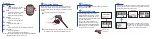
2. NO RASTER (OSD IS NOT DISPLAYED) – LIPS

CHECK MICOM INV

ON/OFF PORT.

J705 PIN2

5V?

NO

NO RASTER

(OSD IS NOT DISPLAYED)

CHECK LIPS

J705 

PIN5, PIN6

5V?

NO

1. CONFIRM BRIGHTNESS

OSD CONTRL STATE.

2. CHECK MICOM DIM-ADJ 

PORT

J705 PIN1

5V?

NO

LIPS

CHECK 

PULSE AS 

CONTACTING SCOPE 

PROBE TO CAUTION LABEL.

(CONTACT PROBE TO 

CAUTION LABEL.

CAN YOU SEE PULSE 

AT YOUR 

SCOPE?

NO

REPLACE CCFL LAMP

IN THE LCD MODULE

YES

YES

YES

YES

Summary of Contents for FLATRON L1530S

Page 1: ...MANUAL Website http biz LGservice com E mail http www LGEservice com techsup html CAUTION BEFORE SERVICING THE UNIT READ THE SAFETY PRECAUTIONS IN THIS MANUAL CHASSIS NO CL 61 MODEL L1530S L1530SM AL R L1530S L1530SSNTM AL R Same model for Service ...

Page 2: ... 1 ...

Page 3: ...Input Voltage Level Low 0 0 8V High 2 1 5 5V 3 Sync Polarity Positive or Negative 3 2 Video Input Signal 1 Type R G B Analog 2 Voltage Level 0 0 7 V a Color 0 0 0 Vp p b Color 7 0 0 35 Vp p c Color 15 0 0 7 Vp p 3 Input Impedance 75 Ω 3 3 Operating Frequency Horizontal 30 63kHz Vertical 56 75Hz 4 POWER SUPPLY 4 1 Power 100 240V 50 60Hz 0 6A 4 2 Power Consumption 5 ENVIRONMENT 5 1 Operating Tempera...

Page 4: ... such as pencil or pen as this may result in damage to the panel Protect the module from the ESD as it may damage the electronic circuit C MOS Make certain that treatment person s body are grounded through wrist band Do not leave the module in high temperature and in areas of high humidity for a long time The module not be exposed to the direct sunlight Avoid contact with water as it may a short c...

Page 5: ...lution 640 x 350 720 x 400 640 x 480 640 x 480 640 x 480 640 x 480 800 x 600 800 x 600 800 x 600 800 x 600 832 x 624 1024 x 768 1024 x 768 1024 x 768 Total Period E 800 449 900 449 800 525 864 525 832 520 840 500 1024 625 1056 628 1040 666 1056 625 1152 667 1344 806 1328 806 1312 800 Video Active Time A 640 350 720 400 640 480 640 480 640 480 640 480 800 600 800 600 800 600 800 600 832 624 1024 76...

Page 6: ...LOCKED should appear You can unlock the OSD controls at any time by pushing the MENU button for 5 seconds The message OSD UNLOCKED should appear 4 Buttons Use these buttons to select or adjust functions in the On Screen Display Button LightView hot key For more information refer to page A13 5 SET AUTO Button Use this button to enter a selection in the On Screen Display AUTO IMAGE ADJUSTMENT When a...

Page 7: ... 6 M M S T 9 1 5 1 J702 J707 Main Board Power Board Control Board J1 J706 WIRING DIAGRAM ...

Page 8: ...AM D SUB MST9011B including ADC LVDS SCALER MTV312 Micom LCD Module R G B differential LVDS Low Voltage Differential Signaling LIPS 5V 5V AC Input 3 3V Reg Diode KDS184 5V 3 3V 12V R G B H V Sync 3 3V 2 5V 3 3V 2 5V ...

Page 9: ...rpolates input to 1280 X 768 resolution signal and outputs 8 bit R G B signal to transmitter 2 Power Part This part consists of the one 3 3V regulator and two 2 5V drop diodes to convert power which is provided 12V 5V in Power board 5V is provided for LCD panel and Micom Also 5V is converted 3 3V by regulator and 3 3V is converted 2 5V by drop diode Converted power is provided for IC in the main b...

Page 10: ... bridge rectifier and a bulk capacitor 3 Energy Transfer This part function is for transfer the primary energy to secondary through a power transformer 4 Output rectifier and filter This part function is to make a pulse width modulation control and to provide the driver signal to power switch to adjust the duty cycle during different AC input and output loading condition to achieve the dc output s...

Page 11: ... is available to LCD Monitor only 1 Port Setup a Copy UserPort sys file to c WINNT system32 drivers folder b Run Userport exe c Remove all default number d Add 300 3FF e Click Start button f Click Exit button 2 EDID Read Write 1 Run WinEDID exe 2 Edit Week of Manufacture Year of Manufacture Serial Number a Input User Info Data b Click Update button c Click Write button ...

Page 12: ...nt side of display 2 Wait for about 5 seconds and press MENU POWER key 3 Shows the service OSD menu 4 The service OSD menu contains additional menus that the User OSD menu as described below a CLEAR ETI To initialize using time b AUTO COLOR W B balance and Automatically sets the gain and offset value c AGING Select Aging mode on off d PANEL Select using panel e NVRAM INIT EEPROM initialize 24C08 f...

Page 13: ...UT A SHORT POINT AS OPENING EACH POWER LINE CHECK J705 VOLTAGE PIN5 PIN6 5V NO CHECK 5VS LINE OPEN CHECK CHECK U501 PIN 8 Voltage 5V NO NO NO CHECK U201 PIN 122 PULSE CHECK U201 CHECK 3 3V LINE CHECK X TAL IS U201 PIN114 3 3V VOLTAGE YES YES NO PROBLEM YES CHECK KEY CONTROL CONNECTOR ROUTINE YES ...

Page 14: ...NOT DISPLAYED CHECK LIPS J705 PIN5 PIN6 5V NO 1 CONFIRM BRIGHTNESS OSD CONTRL STATE 2 CHECK MICOM DIM ADJ PORT J705 PIN1 5V NO LIPS CHECK PULSE AS CONTACTING SCOPE PROBE TO CAUTION LABEL CONTACT PROBE TO CAUTION LABEL CAN YOU SEE PULSE AT YOUR SCOPE NO REPLACE CCFL LAMP IN THE LCD MODULE YES YES YES YES ...

Page 15: ...TROUBLE IN U201 U201 POWER PIN8 114 3 3V NO CHECK U801 U201 PIN122 123 OSCILLATE AS 12MHZ CHECK CONNECTION LINE FROM D SUB TO U501 TROUBLE IN CABLE OR LCD MODULE YES YES YES NO RASTER OSD IS NOT DISPLAYED U501 PIN43 IS 48KHz H SYNC PIN44 IS 60Hz V SYNC IS PULSE APPEARED AT SIGNAL PINS AT MODE 12 NO NO ...

Page 16: ... 15 4 TROUBLE IN DPM TROUBLE IN DPM TROUBLE IN U501 CHECK PC PC IS NOT GOING INTO DPM OFF MODE NO CHECK H V SYNC LINE NO YES YES CHECK R773 R775 SYNC CHECK U501 PIN 43 44 SYNC PULSE ...

Page 17: ... 16 EXPLODED VIEW 1 3 2 5 6 6 9 12 13 8 10 7 4 1 11 2 11 1 4 2 ...

Page 18: ... ASSEMBLY FRAME L1530 _LPL_ANALOG AUO L1530S 4951TKS136B METAL ASSEMBLY FRAME L1530_HANSTAR_ANALOG L1530S 4951TKS136J METAL ASSEMBLY FRAME A CKD L1530S SNT 4814TKK263A SHIELD INVERTER CAP L1530 6871TPT271N PWB PCB ASSEMBLY POWER M CHASSIS 15INCH POWER TOTAL LIEN CHANG C306 68PF LPL HannStar 6871TPT271A PWB PCB ASSEMBLY POWER 15 M CHASSIS POWER TOTAL LIEN CHANG A INTEGRATED LIPS AUO 3313TL5090A MAI...

Page 19: ...0 R TP X7R C735 0CK104CK56A 0 1UF 1608 50V 10 R TP X7R C760 0CE107EF610 100UF KMG RD 16V 20 FL BULK C801 0CK103CK51A 0 01UF 1608 50V 10 R TP B Y5 C803 0CE107EF610 100UF KMG RD 16V 20 FL BULK DATE 2004 3 23 S AL LOC NO PART NO DESCRIPTION SPECIFICATION C804 0CK104CK56A 0 1UF 1608 50V 10 R TP X7R C805 0CK104CK56A 0 1UF 1608 50V 10 R TP X7R C806 0CK103CK51A 0 01UF 1608 50V 10 R TP B Y5 C807 0CE107EF6...

Page 20: ...75 OHM 1 10 W 5 1608 R TP R708 0RJ4700D677 470 OHM 1 10 W 5 1608 R TP R709 0RJ1001D677 1K OHM 1 10 W 5 1608 R TP R716 0RJ4701D677 4 7K OHM 1 10 W 5 1608 R TP R717 0RJ4701D677 4 7K OHM 1 10 W 5 1608 R TP R722 0RJ1000D677 100 OHM 1 10 W 5 1608 R TP R723 0RJ0332D677 33 OHM 1 10 W 5 1608 R TP R724 0RJ0332D677 33 OHM 1 10 W 5 1608 R TP R726 0RJ1002D677 10K OHM 1 10 W 5 1608 R TP R727 0RJ1002D677 10K OH...

Page 21: ...SCHEMATIC DIAGRAM 20 1 H V SYNC DETECT 1 ...

Page 22: ... 21 2 AMP TMDS 2 ...

Page 23: ... 22 3 VIDEO PROCESSOR 3 ...

Page 24: ... 23 4 OUT PUT 4 ...

Page 25: ...Mar 2004 P NO 3828TSL084K Printed in Korea ...

Reviews: