


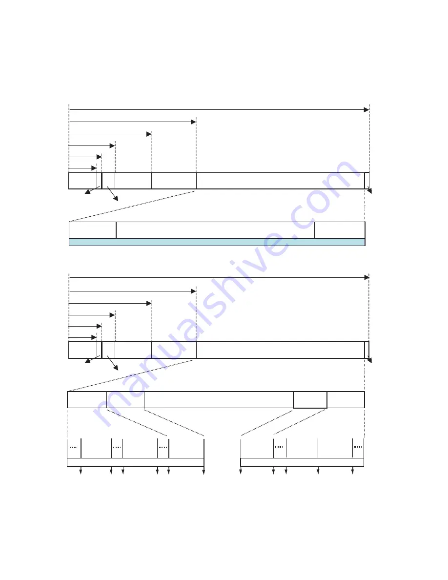
4-39
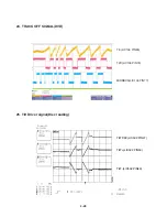
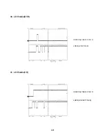
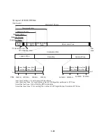
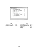
Inner Disc Test Zone : fo r performing OPC procedures.
Inner Disc Count Zone : For counting the nu mber of OPC algorithm performed in IDT Zone.
Outer Disc Test Zone :
for performing OPC procedures.
Outer Disc Count Zone :
For counting t he number of OPC algorithm perf ormed in IDT Zone.
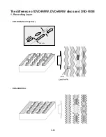
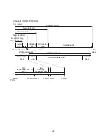
2) Layout of DVD+R disc
1) Layout of DVD-ROM disc
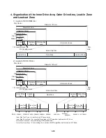
Inform ation Zone
Center
hole
Clamping
Zone
Diameter 120 mm
Diameter 15mm
Data Zone
Lead-in Zone
Lead-out Zone
Read Only Disc
Disc Center
Diameter 16mm
Diameter 22mm
3th tra nsition
area
Diameter 33mm
Diameter 44mm
1th tra nsition area
2th transition area
Rim
area
Data Zone
Lead-in
Zone
In ner Drive
Area
Unrecorded Disc
Outer Drive
Area
Inner Disc
Test Zone
in
27080H
28480H
Inform ation Zone
Center
hole
Clamping
Zone
Diameter 120 mm
Diameter 15mm
Disc Center
Diameter 16mm
Diameter 22mm
3th tra nsition
area
Diameter 33mm
Diameter 44mm
1th tra nsition area
2th transition area
Rim
area
Lead-out
Zone
23080H
PSN :
Inner Disc
Count Zone
27480H
2A480H 30000H
out
Outer Disc
Test Zone
261940H
263940H
260540H
Outer Disc
Count Zone
262940H
267940H
4. Organization of the Inner Drive Area, Outer Drive Area, Lead-in Zone
and Lead-out Zone
Summary of Contents for 7823W
Page 41: ...3 42 3 43 2 E5 BGA POWER UART2_RS232C CIRCUIT DIAGRAM A B C D E F G H I J K L M N O P Q R S T ...
Page 45: ...3 50 3 51 A B C D E F G H I J K L M N O P Q R S T 6 VIDEO DECODER IO JACK CIRCUIT DIAGRAM ...
Page 46: ...3 52 3 53 7 ATAPI 1 2 MEMORY CARD I O CIRCUIT DIAGRAM A B C D E F G H I J K L M N O P Q R S T ...
Page 47: ...3 54 3 55 8 JACK CIRCUIT DIAGRAM A B C D E F G H I J K L M N O P Q R S T ...
Page 48: ...3 56 3 57 9 I O µ COM CIRCUIT DIAGRAM A B C D E F G H I J K L M N O P Q R S T ...
Page 49: ...3 58 3 59 10 TUNER MPX ADC DAC JACK CIRCUIT DIAGRAM A B C D E F G H I J K L M N O P Q R S T ...
Page 50: ...3 60 3 61 11 KEY CIRCUIT DIAGRAM 5 TOOL ONLY A B C D E F G H I J K L M N O P Q R S T ...
Page 51: ...12 KEY CIRCUIT DIAGRAM 6 TOOL ONLY A B C D E F G H I J K L M N O P Q R S T 3 62 3 63 ...
Page 52: ...3 64 3 65 13 KEY CIRCUIT DIAGRAM 8 TOOL ONLY A B C D E F G H I J K L M N O P Q R S T ...
Page 53: ...14 KEY CIRCUIT DIAGRAM 9 TOOL ONLY A B C D E F G H I J K L M N O P Q R S T 3 66 3 67 ...
Page 54: ...3 68 3 69 15 TIMER CIRCUIT DIAGRAM 5 TOOL ONLY A B C D E F G H I J K L M N O P Q R S T ...
Page 55: ...3 70 3 71 16 TIMER CIRCUIT DIAGRAM 6 TOOL ONLY A B C D E F G H I J K L M N O P Q R S T ...
Page 56: ...3 72 3 73 17 TIMER CIRCUIT DIAGRAM 8 TOOL ONLY A B C D E F G H I J K L M N O P Q R S T ...
Page 57: ...3 74 3 75 18 TIMER CIRCUIT DIAGRAM 9 TOOL ONLY A B C D E F G H I J K L M N O P Q R S T ...
Page 62: ...3 84 3 85 PRINTED CIRCUIT DIAGRAMS 1 MAIN P C BOARD TOP SIDE LOCATION GUIDE ...
Page 63: ...3 86 3 87 LOCATION GUIDE 2 MAIN P C BOARD BOTTOM SIDE ...
Page 64: ...3 88 3 89 3 I O P C BOARD TOP VIEW BOTTOM VIEW 4 JACK P C BOARD ...
Page 65: ...3 90 3 91 6 POWER P C BOARD LOCATION GUIDE BOTTOM VIEW 5 HDD P C BOARD TOP VIEW ...
Page 67: ......
Page 87: ...4 20 9 LASER TURN ON SIGNAL F LIC502 PIN 52 LDEN DVD LCN201 PIN17 VRDC LCN201PIN 34 ...
Page 102: ...4 35 2 Disc Specification 3 Disc Materials 1 DVD ROM Single Layer Dual Layer ...
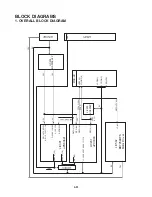
Page 122: ...4 55 4 56 CIRCUIT DIAGRAMS 1 RF CIRCUIT DIAGRAM A B C D E F G H I J K L M N O P Q R S T ...
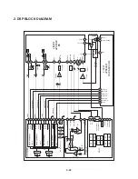
Page 123: ...4 57 4 58 2 DSP CIRCUIT DIAGRAM A B C D E F G H I J K L M N O P Q R S T ...
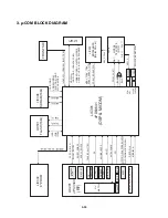
Page 124: ...4 59 4 60 3 µ COM CIRCUIT DIAGRAM A B C D E F G H I J K L M N O P Q R S T ...
Page 126: ...4 63 4 64 PRINTED CIRCUIT DIAGRAMS 1 MAIN P C BOARD LOCATION GUIDE ...


