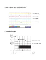
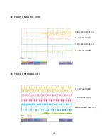


4-38
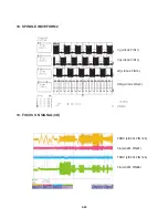
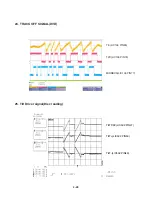
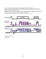
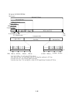
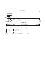
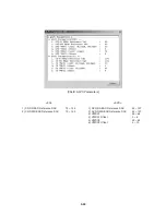
To make recordings, it is necessary to modulate the write pulse, which is called “Write Strategy”.
There can be many types in Write Strategy. Typically Write Strategy for DVD ±R has NMP(Non Multi-Pulse) type and
MP(Multi-Pulse) type. In NMP type each single mark is created by subsequent separated short pulses. In MP type each
single mark is created by one continuous pulse.
Write Strategy for DVD ±RW has Type 1 and Type2. In Type 1 the mark with nT width is created by one top pulse and (n-2)
multi-pulses. Thus mark 3T is made by one top pulse and one multi-pulse. In Type 2 the mark with nT width is created by
one top pulse and (n-3) multi-pulses. Thus mark 3T is made by one top pulse only.
RL-02A uses MP type Write Strategy for DVD ±R and Type 1 for DVD ±RW as shown below.
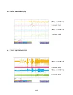
Po :Write Power (Peak Power)
Pe :Erase Power
Pb :Bias Power
Recording data
Twd (3T )
Twd ( 8T )
Ttop
Tmp
Po
Ttop
Zero Level
Pb
Write pulse
for DVD R
Ttop
Ttop
Tmp
Po
Pb
Pe
Write pulse
for DVD RW
Tmp
Zero Level
Tcl
Tcl
Summary of Contents for 7823W
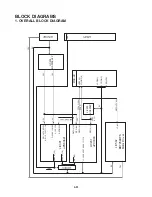
Page 41: ...3 42 3 43 2 E5 BGA POWER UART2_RS232C CIRCUIT DIAGRAM A B C D E F G H I J K L M N O P Q R S T ...
Page 45: ...3 50 3 51 A B C D E F G H I J K L M N O P Q R S T 6 VIDEO DECODER IO JACK CIRCUIT DIAGRAM ...
Page 46: ...3 52 3 53 7 ATAPI 1 2 MEMORY CARD I O CIRCUIT DIAGRAM A B C D E F G H I J K L M N O P Q R S T ...
Page 47: ...3 54 3 55 8 JACK CIRCUIT DIAGRAM A B C D E F G H I J K L M N O P Q R S T ...
Page 48: ...3 56 3 57 9 I O µ COM CIRCUIT DIAGRAM A B C D E F G H I J K L M N O P Q R S T ...
Page 49: ...3 58 3 59 10 TUNER MPX ADC DAC JACK CIRCUIT DIAGRAM A B C D E F G H I J K L M N O P Q R S T ...
Page 50: ...3 60 3 61 11 KEY CIRCUIT DIAGRAM 5 TOOL ONLY A B C D E F G H I J K L M N O P Q R S T ...
Page 51: ...12 KEY CIRCUIT DIAGRAM 6 TOOL ONLY A B C D E F G H I J K L M N O P Q R S T 3 62 3 63 ...
Page 52: ...3 64 3 65 13 KEY CIRCUIT DIAGRAM 8 TOOL ONLY A B C D E F G H I J K L M N O P Q R S T ...
Page 53: ...14 KEY CIRCUIT DIAGRAM 9 TOOL ONLY A B C D E F G H I J K L M N O P Q R S T 3 66 3 67 ...
Page 54: ...3 68 3 69 15 TIMER CIRCUIT DIAGRAM 5 TOOL ONLY A B C D E F G H I J K L M N O P Q R S T ...
Page 55: ...3 70 3 71 16 TIMER CIRCUIT DIAGRAM 6 TOOL ONLY A B C D E F G H I J K L M N O P Q R S T ...
Page 56: ...3 72 3 73 17 TIMER CIRCUIT DIAGRAM 8 TOOL ONLY A B C D E F G H I J K L M N O P Q R S T ...
Page 57: ...3 74 3 75 18 TIMER CIRCUIT DIAGRAM 9 TOOL ONLY A B C D E F G H I J K L M N O P Q R S T ...
Page 62: ...3 84 3 85 PRINTED CIRCUIT DIAGRAMS 1 MAIN P C BOARD TOP SIDE LOCATION GUIDE ...
Page 63: ...3 86 3 87 LOCATION GUIDE 2 MAIN P C BOARD BOTTOM SIDE ...
Page 64: ...3 88 3 89 3 I O P C BOARD TOP VIEW BOTTOM VIEW 4 JACK P C BOARD ...
Page 65: ...3 90 3 91 6 POWER P C BOARD LOCATION GUIDE BOTTOM VIEW 5 HDD P C BOARD TOP VIEW ...
Page 67: ......
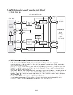
Page 87: ...4 20 9 LASER TURN ON SIGNAL F LIC502 PIN 52 LDEN DVD LCN201 PIN17 VRDC LCN201PIN 34 ...
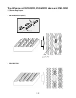
Page 102: ...4 35 2 Disc Specification 3 Disc Materials 1 DVD ROM Single Layer Dual Layer ...
Page 122: ...4 55 4 56 CIRCUIT DIAGRAMS 1 RF CIRCUIT DIAGRAM A B C D E F G H I J K L M N O P Q R S T ...
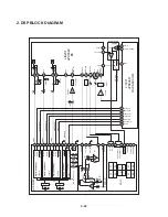
Page 123: ...4 57 4 58 2 DSP CIRCUIT DIAGRAM A B C D E F G H I J K L M N O P Q R S T ...
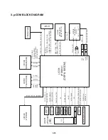
Page 124: ...4 59 4 60 3 µ COM CIRCUIT DIAGRAM A B C D E F G H I J K L M N O P Q R S T ...
Page 126: ...4 63 4 64 PRINTED CIRCUIT DIAGRAMS 1 MAIN P C BOARD LOCATION GUIDE ...


