background image

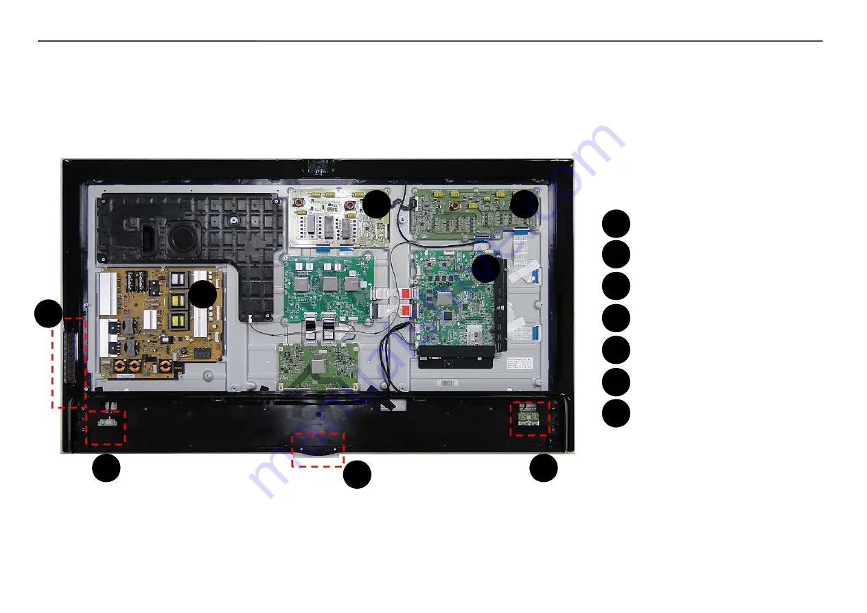
Interconnection - 1

XXLA9700-NA

[PCBs]

7

7

1

Main PCB

2

PSU

1

7

7

3

WIFI ASSY

4

BT MOTION ASSY

1

2

6

5

IR PCB

6

Local Key

5

3

4

7

LED Driver

5

Copyright ⓒ 2013 LG Electronics. Inc. All right reserved.
Only for training and service purposes

LGE Internal Use Only 

Summary of Contents for 65LA9650

Page 1: ...ODEL 65LA9650 65LA9650 UA CAUTION BEFORE SERVICING THE CHASSIS READ THE SAFETY PRECAUTIONS IN THIS MANUAL LED TV SERVICE MANUAL North Latin America http aic lgservice com Europe Africa http eic lgservice com Asia Oceania http biz lgservice com Internal Use Only ...

Page 2: ...Use Only Copyright LG Electronics Inc All rights reserved Only for training and service purposes CONTENTS CONTENTS 2 PRODUCT SAFETY 3 SPECIFICATION 4 ADJUSTMENT INSTRUCTION 14 EXPLODED VIEW 22 SCHEMATIC CIRCUIT DIAGRAM ...

Page 3: ...inals etc to be sure the set is safe to operate without damage of electrical shock Leakage Current Cold Check Antenna Cold Check With the instrument AC plug removed from AC source connect an electrical jumper across the two AC plug prongs Place the AC switch in the on position connect one lead of ohm meter to the AC plug prongs tied together and touch other ohm meter lead in turn to each exposed m...

Page 4: ...lectrostatic charge on your body by touching a known earth ground Alter natively obtain and wear a commercially available discharging wrist strap device which should be removed to prevent poten tial shock reasons prior to applying power to the unit under test 2 After removing an electrical assembly equipped with ES devices place the assembly on a conductive surface such as aluminum foil to prevent...

Page 5: ...he solder joints of the two original leads If they are not shiny reheat them and if necessary apply additional solder Fuse and Conventional Resistor Removal Replacement 1 Clip each fuse or resistor lead at top of the circuit board hollow stake 2 Securely crimp the leads of replacement component around notch at stake top 3 Solder the connections CAUTION Maintain original spacing between the replace...

Page 6: ...er in accordance with BOM 5 The receiver must be operated for about 20 minutes prior to the adjustment 3 Test method 1 Performance LGE TV test method followed 2 Demanded other specification Safety UL CSA CE IEC specification EMC FCC ICES CE IEC specification Wireless Wireless HD Specification Option 4 General Specification No Item Specification Remark 1 Market 1 North America 2 Broad casting Syste...

Page 7: ...50 SDTV DVD 480I 3 720 480 31 50 60 00 27 027 SDTV 480P 4 720 480 31 47 59 94 27 00 SDTV 480P 5 1280 720 45 00 60 00 74 25 HDTV 720P 6 1280 720 44 96 59 94 74 176 HDTV 720P 7 1920 1080 33 75 60 00 74 25 HDTV 1080I 8 1920 1080 33 72 59 94 74 176 HDTV 1080I 9 1920 1080 67 50 60 00 148 50 HDTV 1080P 10 1920 1080 67 432 59 94 148 352 HDTV 1080P 11 1920 1080 27 00 24 00 74 25 HDTV 1080P 12 1920 1080 26...

Page 8: ...A Reduced Blanking O 10 3840 2160 67 5 30 00 297 00 UD 11 3840 2160 56 25 25 00 297 00 UD 12 3840 2160 54 0 24 00 297 00 UD HDMI DTV 1 720 480 31 47 60 27 027 SDTV 480P 2 720 480 31 47 59 94 27 00 SDTV 480P 3 1280 720 45 00 60 00 74 25 HDTV 720P 4 1280 720 44 96 59 94 74 176 HDTV 720P 5 1920 1080 33 75 60 00 74 25 HDTV 1080I 6 1920 1080 33 72 59 94 74 176 HDTV 1080I 7 1920 1080 67 500 60 148 50 HD...

Page 9: ...ve Secondary SDTV 576P SDTV 576P 4 720 576 15 625 50 27 21 Frame packing Field alternative Side by side Full Top and Bottom Side by side half Secondary SDTV 576I SDTV 576I SDTV 576I Secondary SDTV 576I Secondary SDTV 576I 5 1280 720 37 500 50 74 25 19 Top and Bottom Side by side half Primary HDTV 720P Primary HDTV 720P 37 500 50 148 5 19 Side by side Full HDTV 720P 44 96 45 59 94 60 74 17 74 25 4 ...

Page 10: ...TV 1080P 56 250 50 148 5 31 Top and Bottom Side by side half Primary HDTV 1080P Secondary HDTV 1080P 67 43 67 5 59 94 60 148 35 148 50 16 Top and Bottom Side by side half Primary HDTV 1080P Secondary HDTV 1080P 5 2 2 HDMI Input 1 3 No Resolution H freq kHz V freq Hz Pixel clock MHz Proposed 3D input proposed mode 1 720 480 31 5 60 27 03 SDTV 480P 2D to 3D Side by Side Half Top Bottom Checker Board...

Page 11: ...Hz Remark 1 Under 704x480 2D to 3D 2 Over 704x480 interlaced 2D to 3D Side by Side Half Top Bottom 3 Over 704x480 progressive 50 60 2D to 3D Side by Side Half Top Bottom Checker Board Row Interleaving Column Interleaving Frame Sequential 4 Over 704x480 progressive others 2D to 3D Side by Side Half Top Bottom Checker Board Row Interleaving Column Interleaving 5 2 6 USB DLNA Photo Input 3D supported...

Page 12: ...40 2160 54 24 00 296 703 HDTV 2160P 2D to 3D Top Bottom half Side by Side half 56 25 25 00 297 67 5 30 00 296 703 5 Others 27 00 24 00 74 25 640 350 720 400 640 480 800 600 1152 864 2D to 3D Side by Side half Top Bottom 5 2 8 Component Input 3D supported mode manually No Resolution H freq kHz V freq Hz Pixel clock MHz Proposed Remark 1 1280 720 45 00 60 00 74 25 HDTV 720P 2D to 3D Side by Side Hal...

Page 13: ... Miracast Widi 3D supported mode manually No Resolution H freq kHz V freq Hz Pixel clock MHz Remark 1 1024X768p 30 60 2D to 3D Side by Side Half Top Bottom 2 1280x720p 30 60 3 1920X1080p 30 60 4 Others 2D to 3D REMARK 3D INPUT MODE No Side by Side Top Bottom Checkerboard Single Frame Sequential Frame Packing 2D to 3D 1 ...

Page 14: ...stment Component 480i 1080p 2 EDID downloads for HDMI Remark Above adjustment items can be also performed in Final Assembly if needed Adjustment items in both PCBA and final assembly tages can be checked by using the INSTART Menu 1 ADJUST CHECK 3 2 Final assembly adjustment 1 White Balance adjustment 2 RS 232C functionality check 3 Factory Option setting per destination 4 Shipment mode setting In ...

Page 15: ...through information sharing without any necessity of user input It is a realization of Plug and Play 4 4 2 Equipment Since embedded EDID data is used EDID download JIG HDMI cable and D sub cable are not need Adjust remocon 4 4 3 Download method 1 Press Adj key on the Adj R C 2 Select EDID D L menu 3 By pressing Enter key EDID download will begin 4 If Download is successful OK is display but If Dow...

Page 16: ...ms 1 Lighting condition in surrounding area surrounding lighting should be lower 10 lux Try to isolate adj area into dark surrounding 2 Probe location Color Analyzer CA 210 probe should be within 10cm and perpendicular of the module surface 80 100 3 Aging time After Aging Start Keep the Power ON status during 5 Minutes In case of LCD Back light on should be checked using no signal or Full white pa...

Page 17: ... 172 If R gain or G gain is more than 255 G gain can adjust less than 172 and change the others R B Gain Adjustment mode mode Cool 2 Medium Warm Mode Purpose Adjust the color temperature to reduce the deviation of the module color temperature Principle To adjust the white balance without the saturation Fix the one of R G B gain to 192 default data and decrease the others Adjustment mode Two modes ...

Page 18: ...60 277 279 302 304 7 51 80 260 258 275 277 300 302 8 81 119 259 256 274 275 299 300 9 Over 120 259 255 274 274 299 299 5 1 9 V COM Adjust ONLY FOR GP2 2010year model GP3 LW Series 2011year spec out 5 2 Tool Option setting Inspection per countries 5 2 1 Overview 1 Tool option selection is only done for models in Non USA North America due to rating 2 Applied model LA34N Chassis applied to CANADA and...

Page 19: ...by pressing Back Home key of RCU 5 4 3 Applied models Chassis Model Name Magic RF receiver LA34N 55 65LA9700 UA Built in 55 65LA9650 UA 5 5 Wi Fi MAC Address Check 5 5 1 Using RS232 Command Command Set ACK Transmission A l Set ID 20 Cr O K x or N G 5 5 2 Check the menu on in start 5 6 3D pattern test Only for 3D models 5 6 1 Test equipment 1 Pattern Generator MSHG 600 or MSPG 6100 HDMI 1 4 support...

Page 20: ...check how it connects between Camera and PCBA normally and their Function 2 Test Method This Inspection is available only Power Only Status Slide Camera Up Camera s Preview picture apeears on TV Set Slide Camera Down 5 9 Ship out mode check In stop After final inspection press In Stop key of the Adj R C and check that the unit goes to Stand by mode 6 AUDIO output check 6 1 Audio input condition 1 ...

Page 21: ...WER CORD GND and SIGNAL CABLE GND Hi pot Test POWER CORD GND and LIVE NEUTRAL 4 LEAKAGE CURRENT At 0 5mArms 8 USB S W Download optional Service only 1 Put the USB Stick to the USB socket 2 Automatically detecting update file in USB Stick If your downloaded program version in USB Stick is lower than that of TV set it didn t work Otherwise USB data is automatically detected 3 Show the message Copyin...

Page 22: ...Schematic Diagram and EXPLODED VIEW It is essential that these special safety parts should be replaced with the same components as recommended in this manual to prevent X RADIATION Shock Fire or other Hazards Do not modify the original design without permission of manufacturer IMPORTANT SAFETY NOTICE 121 540 521 200 300 541 800 830 570 120 500 560 810 510 330 301 310 820 331 400 320 700 710 590 53...

Page 23: ...PIO64 AR16 SDA1 GPIO79 AP16 SCL2 GPIO78 AP17 SDA2 GPIO77 AR17 SCL3 AP6 SDA3 AR6 SCL4 AH32 SDA4 AJ33 SCL5 AH34 SDA5 AH33 CAM_CE1_N F33 CAM_CE2_N F34 CAM_CD1_N GPIO76 D32 CAM_CD2_N GPIO75 E32 CAM_VS1_N GPIO86 G32 CAM_VS2_N GPIO85 G33 CAM_IREQ_N GPIO73 F32 CAM_RESET G34 CAM_INPACK GPIO74 D33 CAM_VCCEN_N GPIO87 H32 CAM_WAIT_N GPIO84 E33 CAM_REG_N GPIO72 D34 CAM_IOIS16_N GPIO83 H33 SC_CLK GPIO130 T33 S...

Page 24: ...16 AL19 GND_317 AL20 GND_318 AL21 GND_319 AL22 GND_320 AL23 GND_321 AL24 GND_322 AL25 GND_323 AL26 GND_324 AL27 GND_325 AL28 GND_326 AL29 GND_327 AL30 GND_328 AL31 GND_329 AM8 GND_330 AM13 GND_331 AM14 GND_332 AM15 GND_333 AM16 GND_334 AM17 GND_335 AM18 GND_336 AM19 GND_337 AM20 GND_338 AM21 GND_339 AM22 GND_340 AM23 GND_341 AM24 GND_342 AM25 GND_343 AM26 GND_344 AM27 GND_345 AM28 GND_346 AM29 GND...

Page 25: ...7 AUDA_VBG_EXT P2 AUDA_OUTL N1 AUDA_OUTR N2 AUD_SCART_OUTL N3 AUD_SCART_OUTR P1 AUAD_L_CH4_IN P3 AUAD_R_CH4_IN R1 AUAD_L_CH3_IN R2 AUAD_R_CH3_IN T1 AUAD_L_CH2_IN U2 AUAD_R_CH2_IN U3 AUAD_L_CH1_IN V2 AUAD_R_CH1_IN V3 AUAD_R_REF U1 AUAD_M_REF T3 AUAD_L_REF T2 AUAD_REF_PO R3 ANTCON K17 RFAGC K18 IFAGC J18 ADC_I_INCOM U16 ADC_I_INP U17 ADC_I_INN V17 GPIO0 F3 GPIO1 F2 GPIO2 F1 GPIO3 G3 GPIO4 G2 GPIO5 G...

Page 26: ...KN F2 M1_DDR_CKE N5 M1_DDR_ODT G6 M1_DDR_RASN F5 M1_DDR_CASN G5 M1_DDR_WEN H6 M1_DDR_RESET_N K5 M1_DDR_ZQCAL F6 M1_DDR_DQS 0 E2 M1_DDR_DQS_N 0 E1 M1_DDR_DQS 1 F3 M1_DDR_DQS_N 1 F4 M1_DDR_DQS 2 P1 M1_DDR_DQS_N 2 P2 M1_DDR_DQS 3 R3 M1_DDR_DQS_N 3 R4 M1_DDR_DM 0 G4 M1_DDR_DM 1 E3 M1_DDR_DM 2 T4 M1_DDR_DM 3 P3 M1_DDR_DQ 0 C4 M1_DDR_DQ 1 K3 M1_DDR_DQ 2 B3 M1_DDR_DQ 3 J4 M1_DDR_DQ 4 A3 M1_DDR_DQ 5 K2 M1...

Page 27: ...CM_IOWR CI_ADDR 4 R704 10K OPT CI_TS_DATA 0 PCM_IRQA CI_CD1 CI_IN_TS_VAL CI_TS_VAL CI_ADDR 1 CI_ADDR 11 PCM_INPACK CI_VS1 CI_TS_DATA 3 5V_CI_ON CI_TS_DATA 5 R710 0 OPT CI_ADDR 9 R709 10K CI R718 0 OPT CI_TS_DATA 7 5V_CI_ON CI_CD2 R711 10K OPT C706 0 1uF CI CI_DATA 0 7 R707 10K OPT CI_TS_DATA 6 R708 10K OPT CI_TS_DATA 4 CI_TS_SYNC C702 0 1uF CI R712 10K OPT CI_TS_DATA 2 CI_VS1 5V_CI_ON R719 10K OPT...

Page 28: ...PWRGD 15 EN 16 VIN_3 5 AGND 8 RT CLK 6 VSENSE 4 GND_2 2 VIN_2 17 EP GND 3 5V_ST 3 5V_ST R2314 10K 24V PANEL_CTL R2313 1 3K L2320 3 3uH NR5040T3R3N D2300 40V B540C PANEL_VCC PWM_DIM2 1 0V_VDD R2327 1 5 6K 1 PD_20V RL_ON C2306 0 1uF 50V R2326 1 2K 1 PD_ 12V C2330 22uF 10V POWER_ON OFF2_2 C2320 47pF 50V C2331 0 1uF 50V C2346 10uF 10V 3 5V_ST R2302 11K 1 PWM_DIM Q2300 MMBT3906 NXP 1 2 3 R2344 51K 1 C2...

Page 29: ...P27 ANI7 26 P26 ANI6 27 P25 ANI5 28 P24 ANI4 29 P23 ANI3 30 P22 ANI2 31 P21 ANI1 AVREFM 32 P20 ANI0 AVREFP 33 P130 34 P01 TO00 RXD1 35 P00 TI00 TXD1 36 P140 PCLBUZ0 INTP6 37 P120 ANI19 38 P41 TI07 TO07 39 P40 TOOL0 40 RESET 41 P124 XT2 EXCLKS 42 P123 XT1 43 P137 INTP0 44 P122 X2 EXCLK 45 P121 X1 46 REGC 47 VSS 48 VDD IC3000 1 R5F100GEAFB 30 MICOM_LEAD_Cu 1 P60 SCLA0 2 P61 SDAA0 3 P62 4 P63 5 P31 T...

Page 30: ...ET H_SPK_R H_SPK_L H_SPK_L H_SPK_R P3100 SMAW200 H16S2 55 65_Motor 14 GND 9 GND 4 12V 13 SPK_R 8 CTRL_B 3 OPEN_DET 12 GND 7 CTRL_A 2 12V 16 SPK_L 11 SPK_R 6 CTRL_D 1 CLOSE_DET 15 SPK_L 10 GND 5 CTRL_C 17 GND L3100 CIS21J121 IC3100 KID65003AF 55 65_Motor 3 I3 2 I2 4 I4 1 I1 6 I6 5 I5 7 I7 8 GND 9 COMMON 10 O7 11 O6 12 O5 13 O4 14 O3 15 O2 16 O1 IC3101 KID65003AF 55 65_Motor 3 I3 2 I2 4 I4 1 I1 6 I6...

Page 31: ...217 0 1uF 16V VA3203 ESD_HDMI HDMI_CLK HDMI_RX1 I2C_SCL5 IC3200 AZ1117BH 1 2TRE1 1 GND ADJ 2 OUT 3 IN CEC_REMOTE D1 _HDMI3 HDMI_RX2 C3211 0 1uF 16V CK _HDMI1 C3212 1uF 10V D2 _HDMI3 5V_HDMI_2 R3214 33 D1 _HDMI1 D3206 30V MBR230LSFT1G Q3200 MMBT3904 NXP E B C 5V_HDMI_3 C3226 0 1uF 16V OPT D1 _HDMI1 R3220 47K R3233 5 1K 5 1 16W D2 _HDMI2 D0 _HDMI3 DDC_SDA_1 5V_HDMI_3 D2 _HDMI3 D13_HDMI_TX2P D2 _HDMI...

Page 32: ...1 16W 5 R3409 100 1 16W 5 HP_OUT R3403 330K R3404 150 1 10W 5 R3405 150 1 10W 5 C3402 47pF 50V JK3400 PEJ038 4G6 JACK_PARK EAG61030012 3 M3_DETECT 4 M4 5 M5_GND 1 M1 6 M6 JK3403 PEJ038 3B6 EAG61030009 JACK_PARK 3 DETECT 4 L 5 GND 1 R JK3402 PEJ038 4Y6 JACK_PARK EAG61030011 3 M3_DETECT 4 M4 5 M5_GND 1 M1 6 M6 JK3401 JSTIB15 C GND B VCC A VIN 4 SHIELD C3403 0 1uF 16V JK3400 1 KJA PH 1 0177 2 JACK_KS...

Page 33: ...MOTECH CO LTD Q4000 MMBT3904 NXP LOGO_LIGHT E B C L4001 BLM18PG121SN1D R4001 10K LOGO_LIGHT WIFI_DP R4006 100 3 5V_WOL WIFI_DM R4007 100 R4009 10K 5 M_REMOTE_CTS M_REMOTE_RTS LOGO_LIGHT_WAFER R4012 100 LOGO_LIGHT_WAFER P4000 SMAW200 H12S2 WOL RTS TX USB_DM CTS GND 3 3V GND RX 3 5V_WOL RESET USB_DP C4008 47pF 50V C4009 47pF 50V R4014 10K 3 3V_NORMAL C4012 1000pF 50V C4013 47pF 50V OPT C4014 47pF 50...

Page 34: ... 0 1uF CAMERA 3 3V_NORMAL USB2_HUB_IC_IN_DP USB_CAMERA_DM R4204 0 CAMERA CAM_SLIDE_DET C4211 33pF 50V CAMERA R4211 33 CAMERA 3 3V_NORMAL 3 5V_ST RST_HUB USB_CAMERA_DP CAM_CTL R4212 33 CAMERA R4219 10K OPT USB2_HUB_IC_IN_DM C4214 33pF 50V CAMERA R4205 0 CAMERA USB_DM3 R4218 10K CAMERA AUD_LRCK R4217 10K 1 16W 5 CAMERA R4216 100K CAMERA USB_DM3 R4210 0 CAMERA C4201 0 1uF CAMERA AUD_LRCH P4200 12507W...

Page 35: ... 5V_USB_2 5V_NORMAL USB_OCD2 USB_CTL2 R4302 10K USB_CTL3 C4302 0 1uF 16V 3 3V_NORMAL 5V_USB_3 USB_OCD3 R4301 10K USB_DM2 D4300 RCLAMP0502BA 5V_USB_2 USB_DP3 5V_USB_3 JK4300 3AU04S 305 ZC LG 1 2 3 4 5 USB_DM3 USB_DP2 D4302 RCLAMP0502BA JK4302 3AU04S 305 ZC LG 1 2 3 4 5 IC4306 TPS2066CDGNR 3 EN1 2 IN 4 EN2 1 GND 5 FLT2 6 OUT2 7 OUT1 8 FLT1 9 EP GND JK4400 SJ113262 1 VBUS 2 D 3 D 4 GND 5 STDA_SSRX 6 ...

Page 36: ... AUDIO_L_OUT 4 AUDIO_GND 5 B_GND 6 AUDIO_L_IN 7 B_OUT 8 ID 9 G_GND 10 G_OUT 11 R_GND 12 R_OUT 13 RGB_IO 14 SYNC_GND 15 SYNC_OUT 16 SYNC_IN 17 COM_GND 18 AV_DET 19 SHIELD C4803 4700pF EU SC_FB VA4802 5 6V EU L4801 BLM18PG121SN1D EU SC_B SC_R C4804 0 1uF EU SC_ID SC_R_IN R4801 10K EU VA4806 5 6V EU VA4809 5 6V EU SC_L_IN C4802 4700pF EU SC_DET VA4801 5 6V EU DTV MNT_R_OUT C4800 1000pF 50V EU L4800 B...

Page 37: ...P3 TD 4 P4 RD 5 P5 RD 6 P6 CT 7 P7 8 P8 12 SHIELD 9 P9 11 P11 10 P10 GND D1 YL_C D2 YL_A D3 GN_C D4 GN_A EPHY_RDP LAN_JACK_POWER VA5100 5 5V C5100 0 1uF 16V EPHY_TDN JK5100 1 TLA 6T764 LAN_TDK 1 R1 2 R2 3 R3 4 R4 5 R5 6 R6 7 R7 8 R8 12 SHIELD 9 R9 11 R11 10 R10 GND D1 YL_C D2 YL_A D3 GN_C D4 GN_A C5103 0 01uF 50V EPHY_TDP VA5103 5 5V C5101 0 01uF 50V C5102 0 1uF 16V VA5101 5 5V EPHY_RDN R5100 0 50...

Page 38: ...06 33 3 5V_ST Q4300 MMBT3904 NXP E B C C4325 4 7uF 10V R5212 1 5K 1 16W 1 R5204 2 49K 1 EPHY_RDP C5212 0 1uF OPT EPHY_RDN EPHY_TDP IC5200 RTL8201F VB CG 1 RSET 3 MDI 0 7 AVDD33_1 9 RXD 0 10 RXD 1 11 RXD 2 INTB 12 RXD 3 CLK_CTL 13 RXC 14 DVDD33 15 TXC 16 TXD 0 17 TXD 1 18 TXD 2 19 TXD 3 20 TXEN 21 PHYRSTB 22 MDC 23 MDIO 24 LED0 PHYAD 0 PMEB 25 LED1 PHYAD 1 26 CRS CRS_DV 27 COL 28 RXER FXEN 29 DVDD1...

Page 39: ...uF 16V C5629 330pF 50V R5610 470 3 3V_NORMAL R5606 33 24V_AMP WOOFER_MUTE C5616 0 033uF 50V C5637 2200pF 50V IC5600 TAS5733 1 OUT_A 2 PVDD_AB_1 3 PVDD_AB_2 4 BST_A 5 NC_1 6 SSTIMER 7 NC_2 8 PBTL 9 AVSS 10 PLL_FLTM 11 PLL_FLTP 12 VR_ANA 13 AVDD 14 A_SEL_FAULT 15 MCLK 16 OSC_RES 17 DVSSO 18 VR_DIG 19 PDN 20 LRCLK 21 SCLK 22 SDIN 23 SDA 24 SCL 25 RESET 26 STEST 27 DVDD 28 DVSS 29 GND 30 AGND 31 VREG ...

Page 40: ...0V WOOFER_STEREO C5706 0 1uF 16V WOOFER C5736 2200pF 50V WOOFER C5724 0 033uF 50V WOOFER C5703 10uF 10V WOOFER C5738 2200pF 50V WOOFER_STEREO R5710 10K OPT C5701 0 1uF 50V WOOFER C57151uF 25V WOOFER C5734 0 1uF 50V WOOFER_STEREO C5714 0 1uF WOOFER IC5700 TAS5733 WOOFER 1 OUT_A 2 PVDD_AB_1 3 PVDD_AB_2 4 BST_A 5 NC_1 6 SSTIMER 7 NC_2 8 PBTL 9 AVSS 10 PLL_FLTM 11 PLL_FLTP 12 VR_ANA 13 AVDD 14 A_SEL_F...

Page 41: ...2200pF 50V R5805 18K 1 C5827 330pF 50V C5802 10uF 10V H_SPK_L R5806 15K 33 R5803 3 3V_NORMAL C5813 0 1uF R5800 0 C5807 0 047uF C5833 0 1uF 50V AUD_SCK L5805 NRS6045T100MMGK 10 0uH C58141uF 25V C5808 4700pF C5826 330pF 50V C5806 0 1uF C5817 0 1uF 50V L5803 NRS6045T100MMGK 10 0uH R5801 100 C5835 2200pF 50V R5811 18 1 16W C5824 0 033uF 50V GND 5 R5814 18 C5838 2200pF 50V IC5800 TAS5733 Height_SPK 1 O...

Page 42: ...MNT_L_OUT R6002 470K OPT Q6000 MMBT3904 NXP EU E B C R6000 2 2K EU 12V C6007 6800pF OPT SCART_AMP_L_FB R6010 470K OPT C6000 1uF 25V EU R6004 33K EU DTV MNT_R_OUT C6002 6800pF OPT Q6001 MMBT3904 NXP EU E B C L6000 EU SCART_Rout SCART_AMP_R_FB IC6000 AZ4580MTR E1 EU 3 IN1 2 IN1 4 VEE 1 OUT1 5 IN2 6 IN2 7 OUT2 8 VCC R6011 2 2K EU Q6002 RT1P141C T112 EU_SCART_MUTE_ISAHAYA E B C R6014 1K EU R6013 1K EU...

Page 43: ...OUT R6103 33K HP_OUT_MTK C6102 1uF 10V HP_OUT R6105 4 7K HP_OUT C6103 1uF 10V HP_OUT HP_ROUT_MAIN L6100 120 ohm HP_OUT BLM18PG121SN1D C6104 180pF HP_OUT_MTK R6106 43K 1 HP_OUT C6107 0 1uF 16V HP_OUT C6109 180pF HP_OUT_MTK R6102 33K HP_OUT_MTK HP_ROUT_AMP C6104 1 18pF HP_OUT_H13 C6109 1 18pF HP_OUT_H13 C6108 10pF 50V HP_OUT C6106 10pF 50V HP_OUT IC6100 TPA6138A2 3 OUTR 2 INR 4 GND_1 1 INR 6 VSS 5 M...

Page 44: ...NUFATURES SPECFIED PARTS BE USED FOR THE CRITICAL COMPONENTS IN THE SYMBOL MARK OF THE SCHEMETIC 5V_CI_ON 5V_NORMAL R6217 100 CI C6210 1uF 25V CI R6218 10K CI PCM_5V_CTL IC6200 AP2151WG 7 CI 3 FLG 2 GND 4 EN 1 OUT 5 IN R6219 10K CI 62 CI SLOT 2011 10 31 CI POWER ENABLE CONTROL Copyright ⓒ 2013 LG Electronics Inc All right reserved Only for training and service purposes LGE Internal Use Only ...

Page 45: ...4 CGND 15 CLK 16 RST 17 VCC 18 PORADJ 19 CMDVCC 20 RSTIN 21 VDD 22 GND 23 OFF 24 XTAL1 25 XTAL2 26 I OUC 27 AUX1UC 28 AUX2UC R6309 22 JAPAN 3 3V_NORMAL C6300 0 1uF 16V JAPAN C6303 0 1uF 16V JAPAN L6300 BLM18PG121SN1D JAPAN R6312 10K JAPAN R6311 22 JAPAN SMARTCARD_DATA SD_EMMC_CLK C6307 0 33uF 16V JAPAN 5V_NORMAL R6303 OPT 3 3V_NORMAL 3 3V_NORMAL R6304 2 7K JAPAN R6306 OPT R6314 1K JAPAN C6306 0 1u...

Page 46: ...SN1D TU_Q W_KR BR TW CO JP AU Q6501 MMBT3906 NXP TU_A_GLOBAL_6 7 E B C I2C_SCL4_TU R6513 10 TU_Q I2C_SCL4 I2C_SDA4 3 3V_TU R6508 1 1K 5 TU_N M W_TW BR CO C6503 0 1uF 16V TU_S N Q_T US KR TW AU R6502 10 TU_N M S2_RESET_TU R6510 33 NON_TU_W_BR TW CO FE_DEMOD1_TS_DATA 3 LNB_OUT R6531 1 C6531 0 1uF LNB_TX S2_RESET 1 23V_D_Demod C6516 0 1uF 16V TU_N M Q W_KR CN BR JP AU IC6503 AZ1117BH 1 8TRE1 1 ADJ GN...

Page 47: ... B TU_W_JP 1 5V_OR_ 3 3V_SPLITTER 2 RESET_T1 3 SCL_T 4 SDA_T 5 3 3V_T1 6 NC_1 7 1 8V_T1 8 NC_2 9 NC_3 10 NC_4 11 NC_5 12 3 3V_T2 13 1 8V_T2 28 GND_2 29 GND_3 30 B5 1 23V 31 D_RESET 36 LNB 32 B6 3 3V 33 NC_6 34 D_SCL 35 D_SDA GND_4 37 GND_5 38 GND_6 39 TS1_ERROR 40 TS1_SYNC 41 TS1_VALID 42 TS1_MCLK 43 TS1_DATA 44 TS2_ERROR 45 TS2_SYNC 46 TS2_VALID 47 TS2_MCLK 48 TS2_DATA 49 NC_7 50 RESET_T2 51 LNA_...

Page 48: ...68 IC6801 MAX3232CDR EAN41348201 3 C1 2 V 4 C2 1 C1 6 V 5 C2 7 DOUT2 8 RIN2 9 ROUT2 10 DIN2 11 DIN1 12 ROUT1 13 RIN1 14 DOUT1 15 GND 16 VCC 3 5V_ST C6810 0 1uF C6813 0 1uF R6821 100 SOC_RX ZD6803 20V ADUC 20S 02 010L OPT C6809 0 1uF C6812 0 33uF OPT SOC_TX ZD6802 ADUC 20S 02 010L 20V OPT C6811 0 1uF C6808 0 1uF R6820 100 JK6801 SPG13 SD 0402 1 2 3 4 5 6 7 8 9 10 RS 232C Control INTERFACE Copyright...

Page 49: ... LNB_SX34 A_GND A_GND R6903 39K 1 16W 1 LNB A_GND D6903 40V LNB_SMAB34 D6904 40V LNB_SMAB34 LNB_TX C6904 0 1uF 50V LNB C6908 0 1uF LNB C6909 10uF 25V LNB C6912 0 1uF LNB C6902 0 22uF 25V LNB I2C_SCL4 C6900 18pF LNB C6901 33pF LNB IC6900 A8303SESTR T LNB 1 VCP 3 NC_1 7 SCL 9 ADD 10 TONECTRL 11 TCAP 12 ISET 13 VREG 14 GND 15 VIN 16 LX 17 GNDLX 18 NC_2 19 NC_3 20 BOOST 5 TDO 8 SDA 6 IRQ 4 TDI 2 LNB 2...

Page 50: ...NC 3 NC 4 NC 5 NC 6 NC 7 LVDS_SEL 8 NC 9 NC 10 L DIM_ENABLE 11 GND 12 RA0N 13 RA0P 14 RA1N 15 RA1P 16 RA2N 17 RA2P 18 GND 19 RACLKN 20 RACLKP 21 GND 22 RA3N 23 RA3P 24 RA4N 25 RA4P 26 GND 27 BIT_SEL 28 RB0N 29 RB0P 30 RB1N 31 RB1P 32 RB2N 33 RB2P 34 GND 35 RBCLKN 36 RBCLKP 37 GND 38 RB3N 39 RB3P 40 RB4N 41 RB4P 42 GND 43 GND 44 GND 45 GND 46 GND 47 NC 48 VLCD 49 VLCD 50 VLCD 51 VLCD 52 GND PA168_R...

Page 51: ...VSSQ_3 N5 VSSQ_4 P4 VSSQ_5 P6 NC_1 A1 NC_2 A2 NC_3 A8 NC_4 A9 NC_5 A10 NC_6 A11 NC_7 A12 NC_8 A13 NC_9 A14 NC_10 B1 NC_11 B7 NC_12 B8 NC_13 B9 NC_14 B10 NC_15 B11 NC_16 B12 NC_17 B13 NC_18 B14 NC_19 C1 NC_20 C3 NC_22 C7 NC_23 C8 NC_24 C9 NC_25 C10 NC_26 C11 NC_27 C12 NC_28 C13 NC_29 C14 NC_30 D1 NC_31 D2 NC_32 D3 NC_33 D4 NC_34 D12 NC_35 D13 NC_36 D14 NC_37 E1 NC_38 E2 NC_39 E3 NC_40 E12 NC_41 E13...

Page 52: ...12039 0 I2C_SCL2 R12043 1K R12038 0 D13_SPI_DI_M R12042 0 P12002 12507WS 10L 1 2 3 4 5 6 7 8 9 10 11 R12044 0 OPT R12040 0 R12047 0 R12041 0 SPI_DL_MODE R12045 0 OPT D13_SPI_CS GPIO 0 D13_SPI_DO_M IC12000 LG1132 D13 IC_D13 XTALI R2 XTALO R1 PORES_N A18 TRST_N0 E1 TMS0 C3 TCK0 D1 TDI0 B1 TDO0 D3 TRST_N1 E2 TMS1 B3 TCK1 D2 TDI1 B2 TDO1 C2 UART_RXD0 B10 UART_TXD0 A10 UART_RXD1 B9 UART_TXD1 A9 SPI_SCL...

Page 53: ...R12113 1K 1 D13_DDR0_VREFCA D13_DDR0_VREFDQ D13_DDR1_VREFCA D13_DDR1_VREFDQ VDDC15_D13_DDR VDDC15_D13_DDR IC12000 LG1132 D13 IC_D13 DDR_A 0 T11 DDR_A 1 T13 DDR_A 2 T9 DDR_A 3 T7 DDR_A 4 U16 DDR_A 5 U8 DDR_A 6 U15 DDR_A 7 T8 DDR_A 8 T15 DDR_A 9 T10 DDR_A 10 U17 DDR_A 11 U14 DDR_A 12 U13 DDR_A 13 U10 DDR_A 14 T14 DDR_A 15 T12 DDR_BA 0 U7 DDR_BA 1 T16 DDR_BA 2 U11 DDR_U_CK V15 DDR_U_CK_N W15 DDR_D_CK...

Page 54: ...14 DVDD15_DDR_11 P15 DVDD15_DDR_12 P16 DVDD15_DDR_13 P17 DVDD25_OTP J6 AVDD25_HDMI_1 K6 AVDD25_HDMI_2 L6 AVDD25_PLL U2 DVDD33_1 E10 DVDD33_2 E11 DVDD33_3 E12 DVDD33_4 G6 DVDD33_5 J15 DVDD33_6 K15 DVDD33_7 L15 DVDD33_XTAL U1 VREF0_DDR W1 VREF1_DDR W20 VSS_1 A2 VSS_2 A3 VSS_3 A8 VSS_4 A15 VSS_5 A19 VSS_6 B8 VSS_7 B15 VSS_8 B18 VSS_9 B19 VSS_10 B20 VSS_11 C4 VSS_12 C5 VSS_13 C6 VSS_14 C7 VSS_15 C8 VS...

Page 55: ......

Page 56: ...LCD TV Repair Guide p 13 years New Models Applicable Model XXLA9700 NA XXLA9700 NA Copyright ⓒ 2013 LG Electronics Inc All right reserved Only for training and service purposes LGE Internal Use Only ...

Page 57: ...ng g Local dimming depicts more deep black BLU BLU structure Model XXLA9700 NA LED Array is on the side of Module XXLA9700 NA 55inch H 10 V 10 100Block Local Dimming 55inch H 10 V 10 100Block 65inch H 12 V 12 144Block Copyright ⓒ 2013 LG Electronics Inc All right reserved Only for training and service purposes LGE Internal Use Only ...

Page 58: ...36 0mm 전면 Close Open Motor Gear Hinge Motor에서 동력이 전달되면 기어부의 감속 및 구 Gear Gear Link Motor에서 동력이 전달되면 기어부의 감속 및 구 동을 통해 Hinge Gear Link 부에 동력이 전달되면 상 하로 Speaker 가 전달 됨 Speaker Copyright ⓒ 2013 LG Electronics Inc All right reserved Only for training and service purposes LGE Internal Use Only ...

Page 59: ...효과 상하 공간감 기본음이 재생되는 Front 채널과 surround 채널에 Height surround 효과가 인가되어 복합적인 Multi 채널 효과 구현 좌측 Surround 우측 Surround Î UD TV에 걸맞는 multi 채널 음향 구현하여 기존 TV sound와 차별화 가능 Surround Surround 좌측 Front 우측 Front Front Front H i ht Ch l 알고리즘은 청취하는 음악의 음상이 스피커 위치가 아닌 보다 높은 곳에 위치하게 해주는 기술로써 Height Channel 알고리즘은 청취하는 음악의 음상이 스피커 위치가 아닌 보다 높은 곳에 위치하게 해주는 기술로써 기본적으로 사용자 눈높이 혹은 이보다 낮은 곳 에 전면 지향 혹은 하방 지향으로 위치한 스피커의 음상은...

Page 60: ...ng으로 TV off시에도 사운드 강조 디자인 항상 열림 선택 시 Magic Sound Bar 11 TV 켤 때 열림 선택 시 Magic Move 항상 열림 2 1 2 TV on off시 자동으로 speaker 노출 숨김 TV off시 Minimal한 디자인과 TV on 시 장엄한 사운드를 별도 설정 없이 자동 on off TV 켤 때 열림 2 별도 설정 없이 자동 on off Copyright ⓒ 2013 LG Electronics Inc All right reserved Only for training and service purposes LGE Internal Use Only ...

Page 61: ...TRA HD 1 1 Main processor_Digital LG1152D DDR Memory 3 eMMC Memory 2 wifi 2 Main processor_analog LG1152A 4 3 4 Micom for Key IR sensing Audio AMP 50W Motion assy Front Spk 2 5 HDMI switch Local Key IR 5 Copyright ⓒ 2013 LG Electronics Inc All right reserved Only for training and service purposes LGE Internal Use Only ...

Page 62: ... Flash Memory Main B D 1 3 2 Video processor Master PA168 DDR Memory Flash Memory Video processor Slave PA168 3 Power From PSU Module Power To Tcon p DDR Memory Flash Memory Copyright ⓒ 2013 LG Electronics Inc All right reserved Only for training and service purposes LGE Internal Use Only ...

Page 63: ...o_L R AV1_Audio L R AV1 COMP1 AV1_CVBS Comp1 Y Pb Pr Audio AMP SPK I2S COMP1 HDMI Switch HDMI1 3 CI CI HDMI_CEC USB1 USB3 0 Vx1 EPI LVDS Combo USB 3 0 USB 2 0 USB_W iFi PHY RMII LAN WOL WOW FRC TCON Vx1 6 lane EPI 16 lane LVDS Quad USB1 USB3 0 USB2 USB2 0 USB3 USB2 0 USB HUB 16 16 USB 2 0 USB 2 0 USB_CAM 8 8 8 eMMC 8 8 DDR3 DDR3 4Gb 2 1600 DDR3 DDR3 DDR3 DDR3 4Gb 4 1600 Copyright ⓒ 2013 LG Electro...

Page 64: ...KB SRAM 48KB ROM OTP I2Cx10 eMMC DMAC 8ch Timer WDT 1ch L R Audio ADC 24b 48KHz USB3 0 x1 Secure Engine Audio DAC 48KHz I2S I2S SW CVBS 3ch CVBS Encoder 32KBI 32KBD 1MB L2 Slim SPK DivX Bluetooth Digital AMP I2S HPD SPDIF UART OTP Timer SRAM 16KB Digital Audio Output CVBS DAC 5x1ch 1ch Component 2ch CVBS AFE 2 ch 12b 54MHz CVBS Out Mux 10x3ch DE Encoder LVDS Tx e Mux R erlacer b Scaler D CR SW SW ...

Page 65: ...H13 Block diagram Copyright ⓒ 2013 LG Electronics Inc All right reserved Only for training and service purposes LGE Internal Use Only ...

Page 66: ...DVB_SOP AL35 TP_DVB_VAL AM36 TP_DVB_CLK FE_DEMOD1_TS_ERROR FE_DEMOD1_TS_SYNC FE_DEMOD1_TS_VAL FE_DEMOD1_TS_CLK SD_SERIAL_D0 20 FE_DEMOD1_TS_DATA 0 AM35 TP_DVB_DATA0 SD_RESET 31 AG5 GPIO9 S2_RESET M DIF P 10 IF P U17 ADC I INP ADC I INP SD_SCL 34 SD_SDA 35 IC2_SCL4 IC2_SDA4 AP6 SCL3 AR6 SDA3 M_SIF 6 M_CVBS 8 M_IF_AGC 9 M_DIF P 10 M_DIF N 11 H13 LG1154AN _ IF_N TUNER_SIF TU_CVBS IF_AGC U17 ADC_I_INP...

Page 67: ...N COMP2_Y_IN_SOC COMP2_Y_IN_SOC_SOY COMP1_Y Component 1 Phone JACK JK3801 KJA PH 1 0177 2 PB2_IN Y2_IN PR2_IN COMP1_Pb COMP2_PB_IN_SOC COMP1_Pr COMP2_PR_IN_SOC Tuner TU6503 TDSQ H651F TU_CVBS TU_CVBS_SOC TUNER_SIF CVBS_IN1 AAD_ADC_SIF TDSQ H651F FE_DEMOD1_TS_ERROR SYNC VAL CLK FE_DEMOD1_TS_DATA 0 7 H13 LG1154D Copyright ⓒ 2013 LG Electronics Inc All right reserved Only for training and service pur...

Page 68: ...A1 AUD_SCK LRCK LRCH AMP_RESET_N DACLRCK DACLRCH MAIN 4P wafer H13 SCL0 SDA0 LPF GPIO21 WOOFER 4P wafer H13 LG1154 LPF LPF MICOM AMP_MUTE SIDE_HP_MUTE 2P wafer TUNER SIF LPF Tuner IEC958OUT AAD_ADC_SIF HP_L ROUT_MAIN HEADPHONE _ _ AUDA_OUTL PHY0_ARC_OUT_0 TUNER_SIF TPA6138A2 Headphone AMP LPF Phone Jack SPDIF_OUT SPDIF_OUT_ARC LINE OUT Copyright ⓒ 2013 LG Electronics Inc All right reserved Only fo...

Page 69: ...NUC HDMI Out put 8bits SPDIF_OUT_ARC HDMI2 HDMI2 CEC_REMOTE H13 LG1154D_A0 TMDS Link 8bits DDC I2C 2bit I2C_SCL SDA 5 2bits DDC_I2C 2bits CEC_REMOTE HDMI3 HDMI3 TMDS Link 8bits MICOM IC3000 R5F100GEAFB OCP IC3202 TPS2554 MHL_DET CEC_REMOTE DDC_I2C 2bits Copyright ⓒ 2013 LG Electronics Inc All right reserved Only for training and service purposes LGE Internal Use Only ...

Page 70: ...EL LG1154D TCON EPI EPI0A LOCK LOCKn TX0 Vx1 Combo EPI0A EPI1A TX0 TX2 EPI0B EPI1B TX1 TX3 TERM1 TERM2 EPI1B TX3 Copyright ⓒ 2013 LG Electronics Inc All right reserved Only for training and service purposes LGE Internal Use Only ...

Page 71: ... EB_CS2 GPIO92 5V_USB2 USB1 USB3 0 PVR Ready USB3_DP DM USB3_DP0 DM0 USB3_RX0P M USB3_TX0P M USB3_RX0P RX0M USB3_TX0P TX0M OCP USB1 TPS2554 USB_CTL2 HUB_VBUS_CTRL0 USB OCD1 5V_USB1 M_REMOTE_RX TX M_REMOTE_CTS RTS UART1_RXD TXD GPIO15 GPIO18 M_REMOTE_RESET Motion Remote Receiver GPIO13 TPS2554 USB_OCD1 HUB_PORT_OVER0 1 H13 LG1154D UART0_RXD UART0_TXD MICOM R5F100GEAFB SOC_TX SOC_RX SOC_TX SOC_RX 4P...

Page 72: ...FRC B D ULTRA HD Block diagram Copyright ⓒ 2013 LG Electronics Inc All right reserved Only for training and service purposes LGE Internal Use Only ...

Page 73: ... NA PCBs 7 7 1 Main PCB 2 PSU 1 7 7 3 WIFI ASSY 4 BT MOTION ASSY 1 2 6 5 IR PCB 6 Local Key 5 3 4 7 LED Driver 5 Copyright ⓒ 2013 LG Electronics Inc All right reserved Only for training and service purposes LGE Internal Use Only ...

Page 74: ...ding SPK control PCB Assy 3 4 BT MOTION ASSY 5 IR Key PCB WIFI ASSY Sliding SPK unit Local Key Local Key PCB IR PCB WIFI ASSY BT MOTION ASSY To Main 1 To Main Copyright ⓒ 2013 LG Electronics Inc All right reserved Only for training and service purposes LGE Internal Use Only ...

Page 75: ...iewing power auto on off 7 8 C Audio error No audio Normal video 8 9 Wrecked audio discontinuation noise 9 10 Remote control Local switch checking 10 MR13 i h ki 11 D Function error MR13 operating checking 11 11 12 Wifi operating checking 12 13 Camera operating checking 13 13 Camera operating checking 13 14 External device recognition error 14 15 E Noise Circuit noise mechanical noise 15 16 F Exte...

Page 76: ...ck Power Board 24V 12V 3 5V etc Normal voltage Y Replace T con FRC Board or module And Adjust VCOM A18 A1 N Move to No video No audio N N Repair Power Board or parts Check Power Board 24V output A18 Normal voltage Y Replace Inverter or module N End Repair Power Board or parts Always check record S W Version and White Precaution A4 A2 Always check record S W Version and White Balance value before r...

Page 77: ... audio Revised date 2 16 Check various Check and Y A18 Normal voltage Check various voltages of Power Board 3 5V 12V 20V or 24V No Video No audio Check and replace MAIN B D Y N End Replace Power Board and repair parts 2 Copyright ⓒ 2013 LG Electronics Inc All right reserved Only for training and service purposes LGE Internal Use Only ...

Page 78: ...hether other equipments have problem or not By connecting RF Cable at other equipment DVD Player Set Top Box Different maker TV etc N N Check RF Cable Connection Check DVD Player Set Top Box Different maker TV etc SVC Check T ld i Y Close Normal Y A4 1 Reconnection 2 Install Booster S W Version S W Upgrade Bulletin Tuner soldering Y Close Picture Contact with signal distributor N Normal N N Replac...

Page 79: ... error Check error COMPONENT AV HDMI N End Replace module error color input mode Y External device C bl External Input C t Check external R l M i FRC B D Ch k T t tt A8 Cable normal Component error external device and cable Replace Main FRC B D N Request repair Check Test pattern Y External device Check external N for external device cable External device Cable normal HDMI error device and cable R...

Page 80: ... device screen error Color error Check Test pattern For other panel External Input error Connect other external device and cable N Replace Screen Check screen condition by input External Input Component HDMI DVI Check S W Version N Check version Check normal operation of External Input Component RGB and HDMI DVI by connecting Jig pattern Generator Set top Box etc Y Replace Main FRC B D normal Requ...

Page 81: ...igh Check Power cord Check Logo LED Replace Power B D Y OK Replace Main B D Stand By Red or Turn Off Operating Turn Off Check Power cord was inserted properly Measure voltage of each output of Power B D Replace Main B D N Normal A18 Y Normal voltage Replace Main B D Y Y N g Check ST BY 3 5V Replace Power B D N Y Normal voltage A18 Close Replace Power B D 6 Copyright ⓒ 2013 LG Electronics Inc All r...

Page 82: ...EY P ff b REMOTE CONTROL Please refer to the all cases which N l POWEROFF_REMOTEKEY Power off by REMOTE CONTROL POWEROFF_OFFTIMER Power off by OFF TIMER POWEROFF_SLEEPTIMER Power off by SLEEP TIMER POWEROFF_INSTOP Power off by INSTOP KEY POWEROFF_AUTOOFF Power off by AUTO OFF POWEROFF ONTIMER P ff b ON TIMER can be displayed on power off mode Normal POWEROFF_ONTIMER Power off by ON TIMER POWEROFF_...

Page 83: ...reen normal Check user menu Speaker off Off N Check audio B 24V of Power Board Normal voltage Y A20 A21 A18 Speaker off Y Cancel OFF Board N Replace Power Board and repair parts Check Speaker N Replace MAIN Board End Disconnection disconnection Y Replace Speaker 8 Copyright ⓒ 2013 LG Electronics Inc All right reserved Only for training and service purposes LGE Internal Use Only ...

Page 84: ...iscontinuation Noise only for D TV N Normal voltage RF External Input signal normal Replace Main B D N Wrecked audio Discontinuation Noise only for Analog Replace Power B D When RF signal is not received Wrecked audio Discontinuation Noise only for External Input Connect and check N Normal received Request repair to external cable ANT provider Replace Main B D In case of End Connect and check othe...

Page 85: ...or solder Normal operating Check B 3 5V On Main B D Normal Voltage N A18 Check IR Output signal Normal Signal N Y N A22 Y Check R C Operating When turn off light in room Check Replace Baterry of R C Close Check 3 5v on Power B D Replace Power B D or Replace Main B D Power B D don t have problem A18 Repair Replace IR B D Normal operating Close If R C operate Explain the customer cause is interferen...

Page 86: ...ss the wheel Check the INSTART menu RF Receiver ver is 00 00 Y N Check Replace Battery of MR13 Close Y Check Repair RF assy connection A23 Normal operating Close Is show ok message N N Press the back key about 5sec Y RF Receiver ver N Cl A4 N Y Replace MR13 y Close Y is 00 00 Close If you conduct the loop at 3times change the M4 Down load the Firmware INSTART MENUÆ14 RF Remocon TestÆ3 Firmware dow...

Page 87: ...ting error Revised date 12 16 Check the INSTART menu Wi Fi Mac value is NG N Check the Wifi wafer 1pin Normal Voltage N Replace Main B D A24 A4 Y Check Repair Wifi cable Close Y A24 connection A4 Wi Fi Mac value is NG N Close A4 Change the Wifi assy Y 12 Copyright ⓒ 2013 LG Electronics Inc All right reserved Only for training and service purposes LGE Internal Use Only ...

Page 88: ...rating error Revised date 13 16 Check the INSTART menu Camera Ver is NG N Check the Camera wafer P4200 2pin Normal Voltage N Replace Main B D A25 A4 Y Check Repair Camera cable Close Y A25 connection A4 Camera Ver is NG N Close A4 Change the Camera assy Y 13 Copyright ⓒ 2013 LG Electronics Inc All right reserved Only for training and service purposes LGE Internal Use Only ...

Page 89: ...ion Fix information S W Version N Technical information Check input signal Signal input Y External Input and Component Recognition error Replace Main B D S W Version Y N Check and fix external device cable HDMI DVI Optical Recognition error Replace Main B D Fix in accordance with technical information 14 Copyright ⓒ 2013 LG Electronics Inc All right reserved Only for training and service purposes ...

Page 90: ... provide the description M h i l i i t l p p OR If there is a Tak Tak noise from the cabinet refer to the KMS fix information and then proceed as shown in the solution manual For models without any fix information OR Mechanical noise is a natural phenomenon and apply the 1st level description When the customer does not agree apply the process by stage Describe the basis of the description i P t l ...

Page 91: ... 16 Z i h Replace module Zoom part with exterior damage Module damage Cabinet Cabinet damage Replace cabinet Replace remote controller Remote controller Replace remote controller controller damage Stand dent Replace stand dent ep ace sta d 16 Copyright ⓒ 2013 LG Electronics Inc All right reserved Only for training and service purposes LGE Internal Use Only ...

Page 92: ...Vertical Horizontal bar LCD TV ti di A6 7 A Video error _Vertical Horizontal bar residual image light spot LCD TV connection diagram A6 8 A Video error_ Color error Check Link Cable EPI reconnection condition A7 9 Adj A J K A8 9 Adjustment Test pattern ADJ Key A8 10 Appendix Exchange Main Board 1 A 1 5 11 Exchange Main Board 2 A 2 5 Appendix Defected Type caused by T Con Inverter Module 12 Exchang...

Page 93: ...or_ No audio Normal video Checking method in menu when there is no audio A20 20 Voltage and speaker checking method A21 20 Voltage and speaker checking method when there is no audio A21 21 Remote controller operation checking method A22 D Function error 22 Motion Remote operation checking method A23 23 Wifi operation checking method A24 24 Camera operation checking method A25 24 Camera operation c...

Page 94: ...or_No video Normal audio LCD TV 2013 01 31 date A1 Content Check LCD back light with naked eye XXLA9700 NA After turning on the power and disassembling the case check with the naked eye whether you can see light from 2 locations A1 Copyright ⓒ 2013 LG Electronics Inc All right reserved Only for training and service purposes LGE Internal Use Only ...

Page 95: ...nto White Balance of item 6 3 Aft di th R G B GAIN C t l f C l T 1 Press the ADJ button on the remote controller for adjustment 2 Enter into White Balance of item 9 A2 3 After recording the R G B GAIN Cut value of Color Temp Cool Medium Warm re enter the value after replacing the MAIN BOARD 3 After recording the R G B GAIN Cut value of Color Temp Cool Medium Warm re enter the value after replacing...

Page 96: ...symptom Content LCD TV 2013 01 31 TUNER input signal strength checking method ALL MODELS A3 date Content Settings Æ Set up Æ Manual Tuning Æ select channel When the signal is strong use the attenuator 10dB 15dB 20dB etc attenuator 10dB 15dB 20dB etc A3 Copyright ⓒ 2013 LG Electronics Inc All right reserved Only for training and service purposes LGE Internal Use Only ...

Page 97: ...ror symptom Content LCD TV 2013 01 31 LCD TV Version checking method 1 Checking method for remote controller for adjustment ALL MODELS A4 date Content Version Press the IN START with the remote t ll f dj t t controller for adjustment A4 Copyright ⓒ 2013 LG Electronics Inc All right reserved Only for training and service purposes LGE Internal Use Only ...

Page 98: ...UNER checking part ALL MODELS A5 date Content Checking method 1 Check the signal strength or check whether the screen is normal when the external device is connected 2 After measuring each voltage from power supply finally replace the MAIN BOARD g g p pp y y p A5 Copyright ⓒ 2013 LG Electronics Inc All right reserved Only for training and service purposes LGE Internal Use Only ...

Page 99: ...ot A6 Established date Revised Error symptom Content LCD TV 2013 01 31 LCD TV connection diagram 1 A6 date Content ALL MODELS As the part connecting to the external input check the screen condition by signal A6 Copyright ⓒ 2013 LG Electronics Inc All right reserved Only for training and service purposes LGE Internal Use Only ...

Page 100: ...te Revised Error symptom Content LCD TV 2013 01 31 Check Link Cable LVDS reconnection condition A7 date Content ALL MODELS Check the contact condition of the Link Cable especially dust or mis insertion A7 Copyright ⓒ 2013 LG Electronics Inc All right reserved Only for training and service purposes LGE Internal Use Only ...

Page 101: ...V 2013 01 31 Adjustment Test pattern ADJ Key A8 date Content You can view 6 types of patterns using the ADJ Key Checking item 1 Defective pixel 2 Residual image 3 MODULE error ADD BAR SCAN BAR 4 Video error Classification of MODULE or Main B D A8 Copyright ⓒ 2013 LG Electronics Inc All right reserved Only for training and service purposes LGE Internal Use Only ...

Page 102: ...Broken T Con Defect CNT Broken T Con Defect CNT Broken Solder defect CNT Broken Solder defect CNT Broken Abnormal Power Section Solder defect Short Crack Abnormal Power Section Solder defect Short Crack A 1 5 Copyright ⓒ 2013 LG Electronics Inc All right reserved Only for training and service purposes LGE Internal Use Only ...

Page 103: ...tion Abnormal Power Section Solder defect Short Crack Abnormal Power Section Solder defect Short Crack Fuse Open Abnormal power section Abnormal Display Noise GRADATION GRADATION A 2 5 Copyright ⓒ 2013 LG Electronics Inc All right reserved Only for training and service purposes LGE Internal Use Only ...

Page 104: ...ix Exchange Power Board PSU No Light Dim Light Dim Light Dim Light No picture Sound Ok A 3 5 Copyright ⓒ 2013 LG Electronics Inc All right reserved Only for training and service purposes LGE Internal Use Only ...

Page 105: ...damage Panel Mura Light leakage Crosstalk Crosstalk Press damage Un repairable Cases In this case please exchange the module p g Press damage A 4 5 Copyright ⓒ 2013 LG Electronics Inc All right reserved Only for training and service purposes LGE Internal Use Only ...

Page 106: ...Gate TAB IC Defect Gate TAB IC Defect Gate TAB IC Defect Horizontal Block Gate TAB IC Defect Horizontal line Gate TAB IC Defect Un repairable Cases In this case please exchange the module Gate TAB IC Defect Horizontal Block p g Gate TAB IC Defect Gate TAB IC Defect A 5 5 Copyright ⓒ 2013 LG Electronics Inc All right reserved Only for training and service purposes LGE Internal Use Only ...

Page 107: ...Established date Revised Error symptom Content LCD TV 2013 01 31 Check front Power Indicator A17 date Content XXLA9700 NA ST BY condition On or Off Power ON condition Turn Off A17 Copyright ⓒ 2013 LG Electronics Inc All right reserved Only for training and service purposes LGE Internal Use Only ...

Page 108: ... A18 Content Check power input voltage and ST BY 3 5V Check the DC 24V 12V 3 5V Check the DC 24V 12V 3 5V 18 Pin Power Board Main Board 1 Power on 2 INV ON 3 3 5V 4 PDIM 1 5 3 5V 6 PDIM 2 7 GND 8 GND 9 24V 10 24V 11 GND 12 GND 13 12V 14 12V 15 12V 16 24V 17 GND 18 GND A18 Copyright ⓒ 2013 LG Electronics Inc All right reserved Only for training and service purposes LGE Internal Use Only ...

Page 109: ...ised Error symptom Content LCD TV 2013 01 31 POWER OFF MODE checking method ALL MODELS A19 date Content Entry method 1 Press the IN START button of the remote controller for adjustment 2 Check the entry into adjustment item 3 A19 Copyright ⓒ 2013 LG Electronics Inc All right reserved Only for training and service purposes LGE Internal Use Only ...

Page 110: ... 2013 01 31 Checking method in menu when there is no audio ALL MODELS A20 date Content Checking method 1 Press the Setting button on the remote controller g 2 Select the Sound function of the Menu 3 Select the Sound Setting 4 Select TV Speaker p A20 Copyright ⓒ 2013 LG Electronics Inc All right reserved Only for training and service purposes LGE Internal Use Only ...

Page 111: ...GND 8 GND 9 24V 10 24V 11 GND 12 GND 13 12V 14 12V 15 12V 16 24V 17 GND 18 GND Checking order when there is no audio Check the contact condition of or 24V connector of Main Board Measure the 24V input voltage supplied from Power Board If there is no input voltage remove and check the connector Connect the tester RX1 to the speaker terminal and if you hear the Chik Chik sound when you touch the GND...

Page 112: ...T 8 GND Checking order g 1 2 Check IR cable condition between IR Main board 3 Check the st by 3 5V on the terminal 4 7 4 When checking the Pre Amp when the power is in ON condition it is normal when the Analog Tester needle moves slowly and defective when it does not move at all Analog Tester needle moves slowly and defective when it does not move at all A22 Copyright ⓒ 2013 LG Electronics Inc All...

Page 113: ...d date Content A23 XXLA9700 NA 1 3 5V_WOL 2 3 3V 3 USB_DM 4 RTS 5 USB DP 5 USB_DP 6 RX 7 GND 8 TX 9 WOL 9 WOL 10 RESET 11 GND 12 CTS 13 NC 14 3 5V_ST OLED 15 IR OLED 16 GND 16 GND Checking order 1 2 Check Motion cable condition between Motion assy Main board 3 Check the 3 3V on the terminal 2 A23 Copyright ⓒ 2013 LG Electronics Inc All right reserved Only for training and service purposes LGE Inte...

Page 114: ... 3 5V WOL 1 3 5V_WOL 2 3 3V 3 USB_DM 4 RTS 5 USB DP 5 USB_DP 6 RX 7 GND 8 TX 9 WOL 9 WOL 10 RESET 11 GND 12 CTS 13 NC 14 3 5V_ST OLED 15 IR OLED 16 GND Checking order 16 GND Checking order 1 2 Check Wifi cable condition between Wifi assy Main board 3 Check the 3 3V on the terminal 2 A29 Copyright ⓒ 2013 LG Electronics Inc All right reserved Only for training and service purposes LGE Internal Use O...

Page 115: ... DET 1 CAM_SLIDE_DET 2 3 5V_CAM 3 AUD_LRCH 4 AUD_LRCK 5 AUD SCK 5 AUD_SCK 6 GND 7 CAM_PWR_ON_CMD 8 ST_BY_DET_CAM 9 GND 9 GND 10 USB_CAMERA_DP 11 USB_CAMERA_DM 12 GND Checking order Checking order 1 2 Check Camera cable condition between Camera assy Main board 3 Check the 3 5V on the terminal 2 A29 Copyright ⓒ 2013 LG Electronics Inc All right reserved Only for training and service purposes LGE Int...

Page 116: ... TV E Etc 2013 01 31 Tool option changing method A26 date Content XXLA9700 NA Changing method 1 Contact the USB memory USB 1 2 3 jack 2 Enter the password ex 000000 Access USB Memory has each password A30 Copyright ⓒ 2013 LG Electronics Inc All right reserved Only for training and service purposes LGE Internal Use Only ...

Reviews: