- 18 -
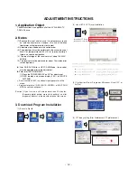
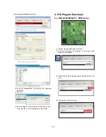
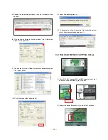
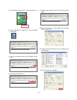
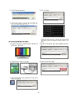
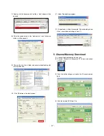
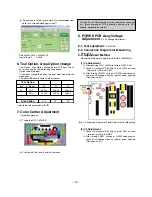
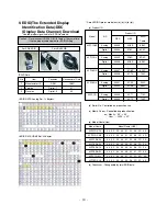
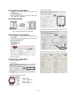
(5) If download is failed, for example “No acknowledge from
slave”, execute download again from(1).
Data 0x00000000 -> 0x000000ff
Num of Byte 0
-> 4096
6. Tool Option, Area Option change
Tool Option, Area Option change Before PCB Assy check,
have to change the Tool option and Area option.
Option value are below.
(If you don’t change the option, the input menu can differ the
model spec.)
The input methods are same as other chassis.
* refer to the Job expression at BOM
7. Color Carrier Adjustment
(Inspection process)
(1) Tuning the RF EU-5CH(C5)
(2) Push the “adj” button at an adjust remocon
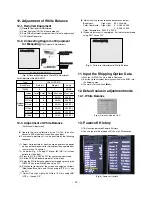
8. POWER PCB Assy Voltage
Adjustment
(Va, Vs Voltage Adjustment)
8-1. Test equipment:
D.M.M 1EA
8-2. Connection Diagram for Measuring
Refer to Fig.1
8-3. Adjustment Method
Adjustment Method for Power Board( P/No: 6709900019A)
(1) Va Adjustment
1) After receiving 100% Full White Pattern, HEAT RUN.
2) C terminal of D.M.M to Va pin of P812, connect
- terminal to GND pin of P812.
3) After turning VR0901, voltage of D.M.M adjustment as
same as Va voltage which on label of panel right/top.
(Deviation; ±0.5V)
(2) Vs Adjustment
1) C terminal of D.M.M to Vs pin of P812, connect
– terminal to GND pin of P812.
2) After turning VR951, voltage of D.M.M adjustment as
same as Va voltage which on label of panel right/top.
(Deviation; ±0.5V)
Tool Option
Inch & Model
42
1RV
3RV
Area Option
Caution: Each PCB assembly must be checked by check JIG
set. (Because power PCB Assembly damages to PDP
Module, especially be careful)
(Fig. 1) Connection Diagram of Power Adjustment for Measuring
ZJ
30224
29200
0~19
TJ
25616
24592
20~
CJ
25616
24592
23
Summary of Contents for 42PC3RA Series
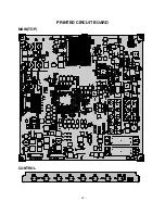
Page 31: ... 31 PRINTED CIRCUIT BOARD MAIN TOP CONTROL ...
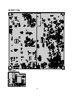
Page 32: ... 32 MAIN BOTTOM PRE AMP ...
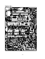
Page 33: ... 33 POWER TOP ...
Page 34: ... 34 POWER BOTTOM ...
Page 35: ... 35 BLOCK DIAGRAM ...
Page 47: ...P No 38549D0018A 1 2 2006 05 30 ...
Page 48: ...P No 38549D0018A 2 2 2006 05 30 ...
Page 49: ...SVC SHEET 38549D0018A S1 ...


