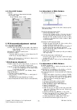


0.1uF
C644
0.1uF
C637
M_SDA
1000pF
C606
22000pF
C616
22000pF
C623
+1.8V_DVDD
1000pF 50V
C651
0.47uF
C632
MULTI_PW_SW
0.1uF
C605
+1.8V_DVDD
0.1uF
C615
0.1uF
C629
AMP_MUTE_HOTEL
+3.3V_MULTI_MST
0.1uF
C643
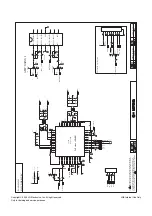
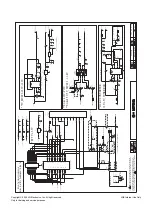
DA-8580
EAP38319001
L607
2S
1S
1F
2F
0.1uF
C617
0.1uF
C602
0.01uF
C647
SPK_R+
M_SCL
0.1uF
C610
DA-8580
EAP38319001
L603
2S
1S
1F
2F
22000pF
C611
SPK_L+
+1.8V_AVDD
SPK_L-
0.1uF
C669
+16V_NTP
+16V_NTP
SPK_R-
100pF
C601
22000pF
C625
+1.8V_AVDD
0.01uF
C672
0.01uF
C648
1000pF
C603
SW_RESET
0.47uF
C673
0.01uF
C671
0.1uF
C626
0.01uF
C613
330uF
35
V
C612
THE SYMBOL MARK OF THIS SCHEMETIC DIAGRAM INCORPORATES
SPECIAL FEATURES IMPORTANT FOR PROTECTION FROM X-RADIATION.
FILRE AND ELECTRICAL SHOCK HAZARDS, WHEN SERVICING IF IS
ESSENTIAL THAT ONLY MANUFATURES SPECFIED PARTS BE USED FOR
THE CRITICAL COMPONENTS IN THE SYMBOL MARK OF THE SCHEMETIC.
SPK_L-
SPK_R+
+1.8V_DVDD
SPK_R-
SMAW250-04
P600
1
2
3
4
SPK_L+
+1.8V_AVDD
+1.8V
I2S_MCLK
I2S_SDO
I2S_WS
I2S_SCK
390pF
C619
390pF
C621
390pF
C630
390pF
C634
1uF
C608
1uF
C618
1uF
C624
1uF
C614
0.1uF
50V
C607
10uF
35V
C642
READY
+12V_AUDIO
MNT_R_AMP
+12V_AUDIO
RT1C3904-T112
Q600
E
B
C
RT1C3904-T112
Q601
E
B
C
MNT_L_AMP
0.01uF
C635
MNT_ROUT
+12V_AUDIO
LM324D
IC601
3
2
INPUT1-
4
VCC
1
OUT1
6
INPUT2-
5
7
OUT2
8
OUT3
9
INPUT3-
10
11
GND
12
13
INPUT4-
14
OUT4
6800pF
C628
6800pF
C627
MNT_LOUT
AUDIO_R
SPK_R-_HOTEL
SPK_R+_HOTEL
12505WR-09A00
HOTEL_OPT
P601
1
2
3
4
5
6
7
8
9
10
0.1uF HOTEL_OPT
C636
+16V_NTP
RT1C3904-T112 HOTEL_OPT
Q602
E
B
C
AMP_MUTE_HOTEL
+3.3V_MULTI_MST
SW_RESET
10uF 16V
C600
10uF 16V
C604
10uF
16
V
C609
3.3
R604
12
R608
12
R611
12
R610
12
R638
4.7K
R663
4.7K
R623
3.3
R626
3.3
R625
100
R601
3.3K
R600
100
R676
100
R677
100
R678
100
R602
100
R603
0
R656
HOTEL_OPT
0
R673
12
R658
12
R653
12
R621
12
R654
4.7K
R628
4.7K
R667
3.3
R671
3.3
R635
1K
R607
10K
NON_HOTEL_OPT
R613
12K
HOTEL_OPT
R613-*
5.6K
R614
5.6K
R615
10K
NON_HOTEL_OPT
R616
12K
HOTEL_OPT
R616-*
1K
R609
4.7K
R606
200
HOTEL_OPT
R612
10K HOTEL_OPT
R617
0
HOTEL_OPT
R620
0
HOTEL_OPT
R619
4.7K
R605
33pF
C631
33pF
C633
0.1uF
C620
0.1uF
C622
6.8K
R618
6.8K
R622
NTP-3100L
IC600
1
BST1A
2
VDR1A
3
RESET
4
AD
5
DVSS_1
6
VSS_IO
7
CLK_I
8
VDD_IO
9
DGND_PLL
10
AGND_PLL
11
LFM
12
AVDD_PLL
13
DVDD_PLL
14
TEST0
15
DVSS_2
16
DVDD
17
SDATA
18
WCK
19
BCK
20
SDA
21
SCL
22
MONITOR_0
23
MONITOR_1
24
MONITOR_2
25
FAULT
26
VDR2B
27
BST2B
28
PGND2B_1
29
PGND2B_2
30
OUT2B_1
31
OUT2B_2
32
PVDD2B_1
33
PVDD2B_2
34
PVDD2A_1
35
PVDD2A_2
36
OUT2A_1
37
OUT2A_2
38
PGND2A_1
39
PGND2A_2
40
BST2A
41
VDR2A
42
NC
43
VDR1B
44
BST1B
45
PGND1B_1
46
PGND1B_2
47
OUT1B_1
48
OUT1B_2
49
PVDD1B_1
50
PVDD1B_2
51
PVDD1A_1
52
PVDD1A_2
53
OUT1A_1
54
OUT1A_2
55
PGND1A_1
56
PGND1A_2
MLB-201209-0120P-N2
0LCML00003B
120-ohm
L605
MLB-201209-0120P-N2
0LCML00003B
120-ohm
L606
33pF 50V
C638
READY
33pF
50V
C639
READY
+3.3V_MST
10K
R630
RT1C3904-T112
Q603
E
B
C
10K
R629
MULTI_PW_SW
0
R627
READY
0
R624
READY
22K
R631
READY
SPK_L-
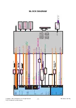
H6 LCD MERCURY
EAX56856904
AUDIO
MSTAR N-EU
2008/12/16
6 9
Main AMP
AMP :GAIN X 4
Chinese Hotel Option
Copyright © 2009 LG Electronics. Inc. All right reserved.
Only for training and service purposes
LGE Internal Use Only
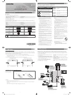
Summary of Contents for 42LH35FR
Page 28: ......