background image

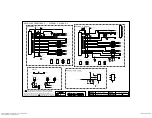
THE    SYMBOL MARK OF THIS SCHEMETIC DIAGRAM INCORPORATES
SPECIAL FEATURES IMPORTANT FOR PROTECTION FROM X-RADIATION.
FIRE AND ELECTRICAL SHOCK HAZARDS, WHEN SERVICING IF IS 
ESSENTIAL THAT ONLY MANUFACTURES SPECIFIED PARTS BE USED FOR
THE CRITICAL COMPONENTS IN THE    SYMBOL MARK OF THE SCHEMETIC.

2 0 1 3 . 0 4 . 2 9

PCMCI

1   o f   1 6

NC5_M1A

Copyright © 2014 LG Electronics. Inc. All rights reserved. 

Only for training and service purposes

LGE Internal Use Only

Summary of Contents for 32LY340C

Page 1: ...ODEL 32LY340C 32LY340C TA CAUTION BEFORE SERVICING THE CHASSIS READ THE SAFETY PRECAUTIONS IN THIS MANUAL LED TV SERVICE MANUAL North Latin America http aic lgservice com Europe Africa http eic lgservice com Asia Oceania http biz lgservice com Internal Use Only ...

Page 2: ...nc All rights reserved Only for training and service purposes CONTENTS CONTENTS 2 SAFETY PRECAUTIONS 3 SERVICING PRECAUTIONS 4 SPECIFICATION 6 ADJUSTMENT INSTRUCTION 9 TROUBLE SHOOTING GUIDE 15 BLOCK DIAGRAM 20 EXPLODED VIEW 21 SCHEMATIC CIRCUIT DIAGRAM ...

Page 3: ...inals etc to be sure the set is safe to operate without damage of electrical shock Leakage Current Cold Check Antenna Cold Check With the instrument AC plug removed from AC source connect an electrical jumper across the two AC plug prongs Place the AC switch in the on position connect one lead of ohm meter to the AC plug prongs tied together and touch other ohm meter lead in turn to each exposed m...

Page 4: ...ctrostatic charge on your body by touching a known earth ground Alter natively obtain and wear a commercially available discharg ing wrist strap device which should be removed to prevent potential shock reasons prior to applying power to the unit under test 2 After removing an electrical assembly equipped with ES devices place the assembly on a conductive surface such as aluminum foil to prevent e...

Page 5: ...he solder joints of the two original leads If they are not shiny reheat them and if necessary apply additional solder Fuse and Conventional Resistor Removal Replacement 1 Clip each fuse or resistor lead at top of the circuit board hollow stake 2 Securely crimp the leads of replacement component around notch at stake top 3 Solder the connections CAUTION Maintain original spacing between the replace...

Page 6: ...1 Performance LGE TV test method followed 2 Demanded other specification Safety CE IEC specification EMC CE IEC 4 Model General Specification No Item Specification Remarks 1 Market Asia Oceania Africa Middle East PAL DVB Market Only Analog for A ASIA 2 Broadcasting system 1 PAL SECAM B G D K 2 PAL I 3 NTSC M 4 DVB T T2 PAL 3 Channel Storage ATV 135 EA DTV 1000 EA 4 Receiving system Analog Upper He...

Page 7: ...50 00 HDTV 1080i 11 1920 1080 33 75 60 00 HDTV 1080i 12 1920 1080 33 72 59 94 HDTV 1080i 13 1920 1080 56 250 50 HDTV 1080p 14 1920 1080 67 5 60 HDTV 1080p 5 2 RGB Input PC No Resolution H freq kHz V freq Hz Pixel clock MHz Proposed Remark 1 640 350 70Hz 31 468 70 09 25 17 EGA 2 720 400 70Hz 31 469 70 08 28 321 DOS 3 640 480 60Hz 31 469 59 940 25 175 VESA VGA 4 800 600 60Hz 37 879 60 31 40 000 VESA...

Page 8: ... 60 053 80 002 VESA O 8 1280 1024 60Hz 63 981 60 020 108 VESA SXGA O FHD only Support to HDMI PC 9 1360 768 60Hz 47 712 60 015 85 5 VESA WXGA O 10 1920 1080 60Hz 67 5 60 0 148 5 WUXGA Reduced blanking O FHD only Support to HDMI PC DTV 1 720 480 31 469 31 5 59 94 60 27 027 SDTV 480P 2 720 576 31 25 50 54 SDTV 576P 3 1280 720 37 500 50 74 25 HDTV 720P 4 1280 720 44 96 45 59 94 60 74 17 74 25 HDTV 72...

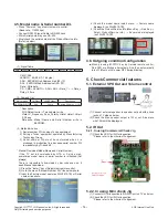
Page 9: ... check OK message If Error is displayed check connection between computer jig and set 3 Click Read tab and then load download file XXXX bin by clicking Read 4 Click Connect tab If Can t is displayed check connection between computer jig and set 5 Click Auto tab and set as below 6 Click Run 7 After downloading check OK message USB DOWNLOAD epk file download 1 Put the USB Stick to the USB socket 2 A...

Page 10: ...y at 8 ADC Calibration Caution Using P ONLY key of the Adjustment remote control power on TV If there is no Component Input disappear ADC Comp message ADC Calibration Protocol RS232 Adjust Sequence aa 00 00 Enter Adjust Mode xb 00 40 Component1 Input 480i ad 00 10 Adjust 480i Comp1 xb 00 60 RGB Input 1024 768 ad 00 10 Adjust 1024 768 RGB aa 00 90 End Adjust mode Required equipment Adjustment remot...

Page 11: ...on Color Temperature COOL Medium Warm One of R Gain G Gain B Gain should be kept on 0xC0 and adjust other two lower than C0 When R G B Gain are all C0 it is the FULL Dynamic Range of Module Mode Temp Coordinate spec Cool 13 000 K X 0 271 0 002 Y 0 270 0 002 Test Signal Inner pattern 204gray 80IRE Medium 9 300 K X 0 286 0 002 Y 0 289 0 002 Warm 6 500 K X 0 313 0 002 Y 0 329 0 002 GP4 Aging time Min...

Page 12: ... y target i First decrease B so make y a little more than the target ii Adjust x value by decreasing the R x target y target i First decrease B so make x a little more than the target ii Adjust x value by decreasing the G After You finish all adjustments Press In start button and compare Tool option and Area option value with its BOM if it is correctly same then unplug the AC cable If it is not sa...

Page 13: ...ufacturer ID GSM 1E6D 2 Version Digital 1 01 3 Revision Digital 3 03 0 1 2 3 4 5 6 7 8 9 A B C D E F 0 0 ff ff ff ff ff ff 0 1e 6d a b 10 c 01 03 68 a0 5a 78 0a ee 91 a3 54 4c 99 26 20 0f 50 54 a1 08 00 71 40 61 40 45 40 31 40 01 01 30 01 01 01 01 01 01 1b 21 50 a0 51 00 1e 30 48 88 40 35 00 40 84 00 00 00 1c 01 1d 00 72 51 d0 1e 20 50 6e 28 55 00 a0 5a 00 00 00 1e 00 00 00 fd 00 3a 60 3e 1e 53 10...

Page 14: ...initialized Not always There is impossible to download by bar code scan so It need Manual download 1 Press the Instart key of Adjustment remote control 2 Go to the menu 6 Model Number D L like below photo 3 Input the Factory model name ex 32LV2510 TB or Serial number like photo 4 Check the model name Instart menu Factory name displayed ex 32LV2510 TB 5 Check the Product Service Info Menu Key Red K...

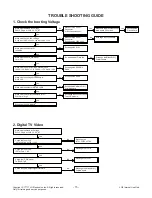
Page 15: ...re the output of MSTAR LVDS Make sure the Inverter controland error P401 2pin High Exchange the LCD Module Make sure the Power Connector Exchange the L402 L403 Exchange the X101 Re download of Firmware Exchange the IC400 3 4 Q406 Exchange the Q409 Exchange the Mstar IC101 Or Main board Exchange the circuit or check The LCD module No No No No No No No No Yes Yes Yes Yes Yes Yes Yes Yes Yes Yes No E...

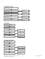
Page 16: ...e and Our TV can support the signal Check the AV cable defect or status of conductor Make sure the JK2802 CVBS signal Make sure the CVBS_DET signal R2812 Make sure the LVDS output signalof Mstar IC Exchange the AV Jack Exchange the R 2810 R2812 Exchange the Mstar IC101 Or Main board No No No Yes Yes Yes Yes 4 AV Video Make sure the input signaltype and Our TV can support the signal Check the Compo...

Page 17: ...output signalof Mstar IC Exchange the Mstar IC101 Or Main board No 6 RGB Video Make sure the input signaltype and Our TV can support the signal Check the HDMI cable defect or status of conductor Check the EDID I2C signal HDMI1 R810 SDA R811 SCL HDMI2 R815 SDA R816 SCL Check the HDMI Jack JK800 JK801 Check the HDMI_DET HPD signal Exchange the IC or download The EDID data Exchange the HDMI Jack Exch...

Page 18: ... No No No Yes Yes Yes Yes Yes Yes Yes Check the Audio output signal IC501 20 21 22 4pin Exchange the Audio AMP IC3400 No Check the connectorP3401 Exchange the connector If the connectoris defect No Check the Speakerresistoror connector Exchange the speaker No Menu toggle No Exchange the AMP IC or Main board No 8 Audio of All input Check the RF cable of RF signal Check the voltage of Tuner 3 3V L37...

Page 19: ...AV cable is defective Check the signalof JK2802 R2805 R2806 Yes Yes Exchange the AV Jack No Implement the 8 Audio of all input Of Malfunction guide 10 AV Audio Check the Component cable is defective Check the signalof JK2800 Yes Yes Exchange the RGDJack No Implement the 8 Audio of all input Of Malfunction guide 11 RGB Audio ...

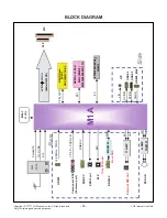
Page 20: ...T MX25L8006EM2I 12G LVDS 80MHz 60Hz HD FHD A AMP TAS5733 USB2 0 DP DM SPK L R X tal 24MHz 51P I2S L R RGB H V RS232C Rear TMDS SPI Component AV Common port Side NAND Flash 1GBIT H27U1G8F2CTR BC PCM_A 0 7 TMDS HDMI2_MHL Y Pb Pr CVBS L R AT24C256C SSHL T 256KBIT I2C TI AMP External SPK Out I2S L R 30P IRout Path SPDIF out H P L R USB2 0 DP DM RJP RJP Only US model 148 5MHz MAX3232 BLOCK DIAGRAM ...

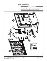
Page 21: ...d mechanical parts in this chassis have special safety related characteristics These parts are identified by in the Schematic Diagram and EXPLODED VIEW It is essential that these special safety parts should be replaced with the same components as recommended in this manual to prevent X RADIATION Shock Fire or other Hazards Do not modify the original design without permission of manufacturer IMPORT...

Page 22: ...0L Q405 G D S 0 1uF 16V C437 27K R427 PD_ 24V 5 1K R428 PD_ 24V THERMAL TPS65282REGR IC400 1 EN 3 SS 7 FAULT2 9 SW_OUT2 10 RLIM 11 AGND 12 SW_OUT1 13 SW_IN_1 14 SW_IN_2 15 FB 16 LX_1 17 LX_2 18 BST 19 PGND_1 20 PGND_2 21 VIN_1 22 VIN_2 23 PGOOD 24 V7V 5 EN_SW2 8 FAULT1 6 EN_SW1 4 ROSC 2 COMP 25 EP GND THERMAL TPS5432DDAR IC403 3 PH 2 VIN 4 GND 1 BOOT 5 VSENSE 6 COMP 7 EN 8 SS 9 EP GND AZ1117EH ADJ...

Page 23: ...al 1 R940 1 eye 22uF 10V C719 18pF 50V C929 Not_eye 0 R941 Not_eye 5V_USB_2 4 7K OPT R713 5V_USB_2 1 R941 1 eye 10K R714 OPT USB2_OCD USB1_CTL 47 R715 OPT RCLAMP0502BA OPT D709 CIS21J121 Wifi Dongle_SS L703 MLB 201209 0120P N2 120 ohm wifi Dongle_MAG L703 1 2pF 50V C929 1 eye USB DOWN STREAM 3AU04S 305 ZC LG JK704 1 2 3 4 5 USB2_DM AP2191DSG EAN61849601 IC702 OPT 3 IN_2 2 IN_1 4 EN 1 GND 5 FLG 6 O...

Page 24: ..._HDMI1_IP4283 3 GND_1 2 TMDS_CH1 4 TMDS_CH2 1 TMDS_CH1 5 TMDS_CH2 6 NC_1 7 NC_2 8 GND_2 9 NC_3 10 NC_4 IP4283CZ10 TBA D804 ESD_HDMI1_IP4283 3 GND_1 2 TMDS_CH1 4 TMDS_CH2 1 TMDS_CH1 5 TMDS_CH2 6 NC_1 7 NC_2 8 GND_2 9 NC_3 10 NC_4 RCLAMP0524PA D803 1 ESD_HDMI1_SEMTECH 1 8 2 7 3 6 4 5 9 10 RCLAMP0524PA ESD_HDMI1_SEMTECH D804 1 1 8 2 7 3 6 4 5 9 10 RCLAMP0524PA ESD_HDMI2_SEMTECH D806 1 1 8 2 7 3 6 4 5...

Page 25: ...A7 R2 A8 T8 A9 R3 A10 AP L7 A11 R7 A12 BC N7 A13 T3 NC_6 M7 BA0 M2 BA1 N8 BA2 M3 CK J7 CK K7 CKE K9 CS L2 ODT K1 RAS J3 CAS K3 W E L3 RESET T2 DQSL F3 DQSL G3 DQSU C7 DQSU B7 D M L E7 D M U D3 DQL0 E3 DQL1 F7 DQL2 F2 DQL3 F8 DQL4 H3 DQL5 H8 DQL6 G2 DQL7 H7 DQU0 D7 DQU1 C3 DQU2 C8 DQU3 C2 DQU4 A7 DQU5 A2 DQU6 B8 DQU7 A3 VREFCA M8 VREFDQ H1 ZQ L8 VDD_1 B2 VDD_2 D9 VDD_3 G7 VDD_4 K2 VDD_5 K8 VDD_6 N1...

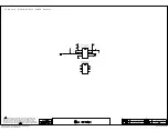
Page 26: ...V_ST 3 5V_ST 0 1uF C1300 4 7K R1301 OPT SPI_CS SPI_SDO MX25L8006EM2I 12G IC1300 SPI_FLASH_MACRONIX 3 WP 2 SO SIO1 4 GND 1 CS 5 SI SIO0 6 SCLK 7 HOLD 8 VCC 33 R1302 10K R1300 OPT SPI_SDI FLASH_WP W25Q80BVSSIG IC1300 1 SPI_FLASH_WINBOND 3 WP IO2 2 DO IO1 4 GND 1 CS 5 DI IO0 6 CLK 7 HOLD IO3 8 VCC 3 5V_ST S e r i a l F l a s h f o r S P I b o o t 2013 04 29 S_FLASH 1 o f 1 6 NC5_S7LR M1A Copyright 20...

Page 27: ... change RXB4 RXACK RXBCK RXA0 RXA2 LVDS RXA2 RXBCK RXB4 RXA3 RXA1 RXB2 RXB3 RXA3 RXBCK RXACK RXA2 RXA1 RXB1 RXB3 RXA3 RXA2 RXA0 RXA4 S h i f t RXBCK RXB2 RXA4 51Pin LVDS Connector For FHD 60Hz RXACK RXA3 RXACK RXB3 RXA3 RXA1 RXB0 RXA0 RXACK RXB3 LVDS_SEL RXA4 RXB3 RXA4 RXA2 RXA2 RXA1 RXB2 Pol change RXB4 RXB1 RXA4 RXACK RXB3 RXB0 RXB3 RXBCK RXB4 RXA0 RXA2 RXB0 RXB1 RXA3 RXA2 RXBCK RXB4 RXA0 RXA4 R...

Page 28: ...D ELECTRICAL SHOCK HAZARDS WHEN SERVICING IF IS ESSENTIAL THAT ONLY MANUFACTURES SPECIFIED PARTS BE USED FOR THE CRITICAL COMPONENTS IN THE SYMBOL MARK OF THE SCHEMETIC 2 0 1 3 0 4 2 9 PCMCI 1 o f 1 6 NC5_M1A Copyright 2014 LG Electronics Inc All rights reserved Only for training and service purposes LGE Internal Use Only ...

Page 29: ...9 PPJ245N2 01 JK2802 5A GN YL O SPRING 6A GN YL E LUG 4A GN YL CONTACT 5B BL O SPRING 7C RD1 E LUG S 5C RD1 O SPRING 4C RD1 CONTACT 5D WH O SPRING 4E RD2 CONTACT 5E RD2 O SPRING 6E RD2 E LUG 20V RGB_VARISTOR VA2809 DSUB_G 20V OPT VA2810 MMBD6100 RGB_PC D2803 A2 C A1 DSUB_R 75 RGB_PC R2820 68pF 50V OPT C2808 20V RGB_VARISTOR VA2808 75 RGB_PC R2818 10K RGB_PC R2823 2 4K R2816 RGB_PC 20V OPT VA2806 5...

Page 30: ...3021 UBW2012 121F L3002 0 47uF 50V EXT_SPK_470nF C3017 HP_LOUT 4 7K EXT_SPK R3020 HP_MUTE 24V 10K OPT R3018 EXT_OUT_R 0 22uF 50V EXT_SPK C3012 HP_ROUT 10K EXT_SPK R3017 TPA3124D2PWPR EXT_SPK IC3000 3 PVCCL_2 2 SD 4 MUTE 1 PVCCL_1 6 RIN 5 LIN 7 BYPASS 8 AGND_1 9 AGND_2 10 PVCCR_1 11 VCLAMP 12 PVCCR_2 13 PGNDR_1 14 PGNDR_2 15 ROUT 16 BSR 17 GAIN1 18 GAIN0 19 AVCC_1 20 AVCC_2 21 BSL 22 LOUT 23 PGNDL_...

Page 31: ... NC_1 6 SSTIMER 7 NC_2 8 PBTL 9 AVSS 10 PLL_FLTM 11 PLL_FLTP 12 VR_ANA 13 AVDD 14 A_SEL_FAULT 15 MCLK 16 OSC_RES 17 DVSSO 18 VR_DIG 19 PDN 20 LRCLK 21 SCLK 22 SDIN 23 SDA 24 SCL 25 RESET 26 STEST 27 DVDD 28 DVSS 29 GND 30 AGND 31 VREG 32 GVDD_OUT 33 BST_D 34 PVDD_CD_1 35 PVDD_CD_2 36 OUT_D 37 PGND_CD_1 38 PGND_CD_2 39 OUT_C 40 NC_3 41 NC_4 42 BST_C 43 BST_B 44 NC_5 45 NC_6 46 OUT_B 47 PGND_AB_1 48...

Page 32: ...3 3 3V 27 SCL_DEMOD 28 B4 1 1V 29 F22_OUTPUT 30 SDA_DEMOD 47 SHIELD B1 B1 A1 A1 22K 1 R3734 0 1uF 16V C3732 3 3V_Normal 22 R3712 0 1uF 16V C3722 100pF 50V C3713 DEMOD_RESET TDJH H101F TU3700 1 TUNER_NTSC 47 SHIELD 6 I F P 7 IF N 8 NC_2 9 NC_3 1 B1 3 3V 2 NC_1 3 IF_AGC 4 SCL 5 SDA A1 A1 B1 B1 0 1uF 16V C3703 0 1uF 16V C3727 1 16W 0 AR3701 T2 3 3V_LNA 12K 1 R3733 47 CHINA AR3701 1 MMBT3906 NXP Q3700...

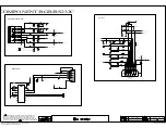
Page 33: ...EMETIC CI_DET DDC_SCL_2 CI_CD1 HP_DET CK _HDMI2 SPDIF_OUT HDMI_ARC D0 _HDMI2 D1 _HDMI2 HP_ROUT D0 _HDMI2 HP_LOUT EPHY_RN EPHY_RP 5V_DET_HDMI_2 HPD2 EPHY_TP D2 _HDMI2 EPHY_TN SENSOR_SDA FRC_RESET D1 _HDMI2 IF_AGC_SEL SENSOR_SCL D2 _HDMI2 CK _HDMI2 DEMOD_RESET DDC_SDA_2 CI_CD2 DSUB_R DSUB_G DSUB_B DSUB_HSYNC DSUB_VSYNC TP for CHINA 2013 04 29 TP_CHINA 1 o f 1 6 NC5_M1A Copyright 2014 LG Electronics ...

Page 34: ... LED_R_Zener VA4600 10K 1 R4604 100pF 50V C4604 1K R4605 EYE_Q SENSOR_SDA 3 3V_Normal 12507WR 08L OPT P4601 1 2 3 4 5 6 7 8 9 0 1uF 16V C4602 BLM18PG121SN1D L4600 18pF 50V C4605 3 5V_ST IR 100 R4609 EYE_Q 3 5V_ST 1 8K R4606 SENSOR_SCL 12507WR 10L P4600 1 2 3 4 5 6 7 8 9 10 11 LED_R BUZZ 2SC3052 Q4601 E B C 1K R4614 3 5V_ST 10K R4613 1K R4612 IR_OUT 47K R4615 22 R4611 3 5V_ST 2SC3052 Q4600 E B C 22...

Page 35: ...G 1 EPI0 GPIO179 N20 LVA0P TTL_G 2 EPI1 GPIO180 N21 LVA0M TTL_G 3 EPI1 GPIO181 N19 LVB4P TTL_G 4 EPI2 GPIO182 M21 LVB4M TTL_G 5 EPI2 GPIO183 M20 LVB3P TTL_G 6 EPI3 GPIO184 M19 LVB3M TTL_G 7 EPI3 GPIO185 L20 LVBCKP TTL_R 0 EPI4 GPIO186 L19 LVBCKM TTL_R 1 EPI4 GPIO187 K20 LVB2P TTL_R 2 EPI5 GPIO188 K21 LVB2M TTL_R 3 EPI5 GPIO189 K19 LVB1P TTL_R 4 EPI6 GPIO190 J21 LVB1M TTL_R 5 EPI6 GPIO191 J20 LVB0P...

Page 36: ...M_1 B5 AVDD_DRAM_2 B6 AVDD_DVI_USB_MPLL_1 R8 AVDD_DVI_USB_MPLL_2 R9 AVDD_MOD_1 L7 AVDD_MOD_2 L8 AVDD_NODIE P8 AVDD_PLL K9 AVDD3P3_DMPLL R5 AVDDL_MOD P11 DVDD_DDR_1 C7 DVDD_DDR_2 M13 DVDD_NODIE R6 DVDD_RX_1_1 A7 DVDD_RX_1_2 M12 DVDD_RX_2_1 B7 DVDD_RX_2_2 M14 VDDC_1 N11 VDDC_2 N12 VDDC_3 N13 VDDC_4 N14 VDDC_5 N15 VDDC_6 P12 VDDC_7 P13 VDDC_8 P14 VDDP L9 AVDD5V_MHL AA10 LGE2131 M1A_128M IC101 1 M1A_1...

Page 37: ......
Reviews: