ML610Q304 Reference Board User’s Manual
FEBL610Q304RB-01
FEBL610Q304-01
13
Page 1: ...chnology and LAPIS Technology succeeded LAPIS Semiconductor s LSI business Therefore all references to LAPIS Semiconductor Co Ltd LAPIS Semiconductor and or LAPIS in this document shall be replaced wi...
Page 2: ...ML610Q304 Reference Board User s Manual 1 st Version Issue date Dec 02 2014 FEBL610Q304 01...
Page 3: ......
Page 4: ...es The Products specified in this document are not designed to be radiation tolerant While LAPIS Semiconductor always makes efforts to enhance the quality and reliability of its Products a Product may...
Page 5: ...s manual provides comprehensive explanation about ML610Q304 Reference Board Together with this manual please also refer to the following documents ML610Q304 User s Manual The manual to explanation abo...
Page 6: ...pply is selectable either from EASE from other board Service pads are provided for mounting additional components that may be necessary to check evaluate Micro s functionalities 1 1 2 Specifications o...
Page 7: ...e Board is as below Figure 1 2 Figure 1 ML610Q304 Reference Board outlook Figure 2 ML610Q304 Reference Board Orientation of mounting IC Cautions Pleases set the IC on the board after turning the power...
Page 8: ...should be turned on after EASE is connected EASE should be put off after the user s sytem is turned off 2 2 VREF jumper VREF jumper is for selecting the line for power supply to VREF pin If supply fro...
Page 9: ...from VDD please set to 1 of SPVDD jumper SP10 If from SPVDD pin please to 3 of SPVDD jumper Figure 5 VREF jumper Cautions When setting to 3 of SPVDD jumper for connecting to EASE please turn on the cu...
Page 10: ...s C9 C11 as appropriate if necessary See Figure 5 below as an example Figure 6 An example of ADC sequential comparator AIN0 AIN2 mounting 2 5 If LED does not emit P20 P22 pins enable direct drive of L...
Page 11: ...10Q304RB 01 FEBL610Q304 01 8 2 6 Cut off power supply Please cut off the patterns of SP1 SP4 VDD SP3 SP6 SPVDD Also please cut SP5 pattern if getting VDDL VSS apart See Figure 7 for an example below F...
Page 12: ...4 P20 CN1 4 Connecting also to LED 5 P80 CN1 5 6 P81 CN1 6 7 TEST1_N Connecting to EASE connector 8 TEST0 Connecting to EASE connector 9 P82 CN2 1 10 P83 CN2 2 11 RESET_N CN2 3 12 SPP CN2 4 Connectin...
Page 13: ...duction and also on the customer s board for massproduciton 4 We do not offer repair service for this board The replacement board will be offered when the failure is notified at early stage 5 Please C...
Page 14: ...0mm Layer two 2 layers Thickness 1 6mm Conductor pitch 2 lines between the pins Conductor width Powerline 0 3mm signal line 0 15mm Rubber cap 4 pieces locations 2 54 15 24 4 3 6 70 1 7 CN3 P42 AIN2 P4...
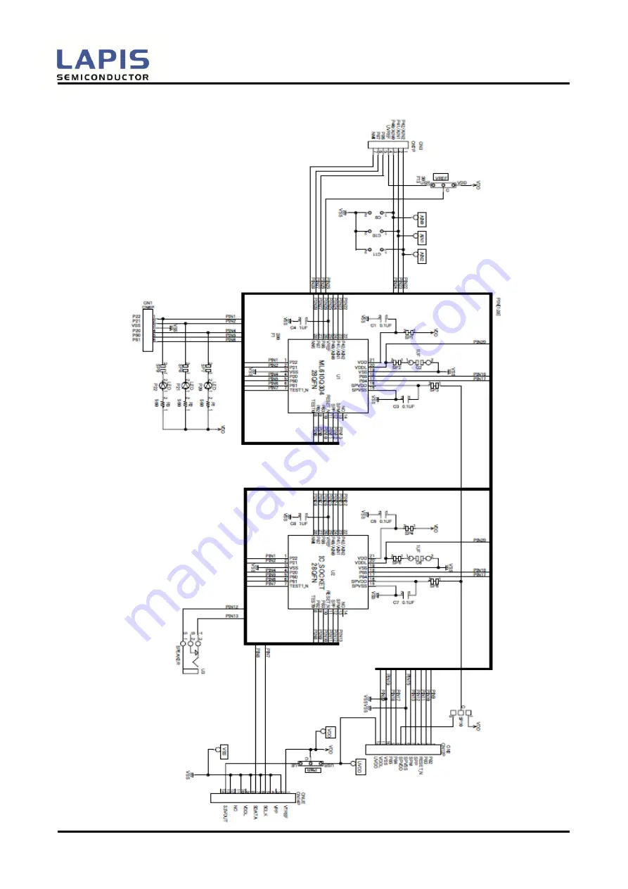
Page 15: ...ML610Q304 Reference Board User s Manual FEBL610Q304RB 01 FEBL610Q304 01 12 5 2 Circuit Diagram Circuit diagram of ML610Q304 Reference Board is show on the next page...
Page 16: ...ML610Q304 Reference Board User s Manual FEBL610Q304RB 01 FEBL610Q304 01 13...
Page 17: ...ML610Q304 Reference Board User s Manual FEBL610Q304RB 01 FEBL610Q304 01 14 Revision history Document No Issue date Page Contents of change Before After FEBL610Q304RB 01 2014 12 2 1 st version issued...