USER GUIDE
www.kontron.com
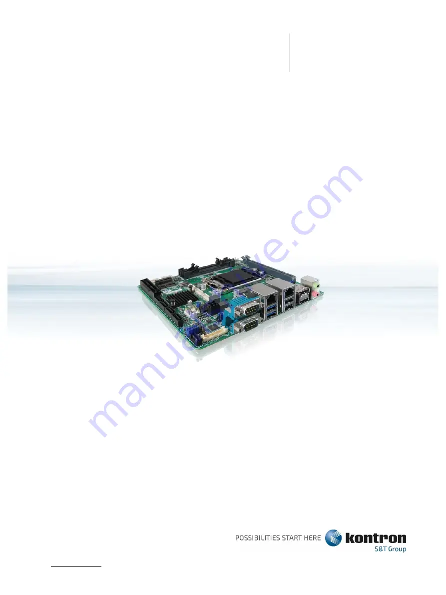
MITX-CFL0 Series
Doc. User Guide, Rev. 1.1
Doc. ID: [To be Determined]
Page 1: ...USER GUIDE www kontron com MITX CFL0 Series Doc User Guide Rev 1 1 Doc ID To be Determined...
Page 2: ...MITX CFL0 Series User Guide Rev 1 1 www kontron com 2 This page has been intentionally left blank...
Page 3: ...n will be suitable for the specified use without further testing or modification Kontron expressly informs the user that this user guide only contains a general description of processes and instructio...
Page 4: ...rely at your risk To minimize the risks associated with your products and applications you should provide adequate design and operating safeguards You are solely responsible for compliance with all le...
Page 5: ...ACT US Customer Support Find Kontron contacts by visiting http www kontron com support Customer Service As a trusted technology innovator and global solutions provider Kontron extends its embedded mar...
Page 6: ...rescribed by the law may endanger your life health and or result in damage to your material ESD Sensitive Device This symbol and title inform that the electronic boards and their components are sensit...
Page 7: ...es before performing any work on this product Earth ground connection to vehicle s chassis or a central grounding point shall remain connected The earth ground cable shall be the last cable to be disc...
Page 8: ...product then re pack it in the same manner as it was delivered Special care is necessary when handling or unpacking the product See Special Handling and Unpacking Instruction Quality and Environmenta...
Page 9: ...ards and Certifications 19 3 5 Processor Support 20 3 6 System Memory Support 20 3 6 1 Memory Operating Frequencies 20 3 7 On board Graphics Subsystem 21 3 8 Power Supply Voltage 21 4 Connector Locati...
Page 10: ...or PCIEX16 PEG_X16_X8 67 7 21 3 Pin 9 Power Selection for COM 5 COM 6 COME_PW COMF_PW 67 7 21 4 Panel Backlight Power Selection for LVDS LCD_VCC 68 7 21 5 Backlight Power Enable Selection for LVDS BL_...
Page 11: ...Assignment M 2 Key E Socket 53 Table 36 Pin Assignment M 2 Key M Socket 56 Table 37 Pin Assignment U_SIM 59 Table 38 Pin Assignment PCIEX16 61 Table 39 Pin Assignment VOLUME_CONTROL 64 Table 40 Pin As...
Page 12: ...in Menu Screen System Data and Time 73 Figure 45 BIOS Advanced Menu 75 Figure 46 BIOS Advanced Menu Display Configuration 76 Figure 47 BIOS Advanced Menu Super IO Configuration 78 Figure 48 BIOS Advan...
Page 13: ...MITX CFL0 Series board s special features and is not intended to be a standard PC AT textbook New users are recommended to study the short installation procedure stated in the following chapter befor...
Page 14: ...tc might get damaged Make sure to use a standard ATX PSU and a standard ATX12V PSU with suitable cable kits and PS ON active The power supply unit shall comply with the requirements as defined in IEC...
Page 15: ...m input current For interfaces having a power pin such as external power or fan ensure that the connectors and wires are suitably rated All connections from and to the product shall be with SELV circu...
Page 16: ...te av batteri Benytt samme batteritype eller en tilsvarende type anbefalt av apparatfabrikanten Brukte batterier kasseres i henhold til fabrikantens instruksjoner VARNING Explosionsfara vid felaktigt...
Page 17: ...MITX CFL0 Series User Guide Rev 1 1 www kontron com 17 3 System Specifications 3 1 System Block Diagram Figure 1 System Block Diagram MITX CFL0 Series...
Page 18: ...nterface 2x Speaker out 3 W by header 2x Line out 1x on rear 1x by header 2x Mic in 1x on rear 1x by header Network Connection Ethernet 2x GbE LAN RJ45 on rear 1x Intel I211 AT 1x Intel I219 LM Q370 I...
Page 19: ...x Header for Reset button HDD LED External Speaker 1x Header for Power button Power LED SM bus 1x Header for Volume Control 1x Header for Chassis Intrusion Detection Cooling Cooling Method 1x Wafer fo...
Page 20: ...ase load of processor 3 6 System Memory Support The MITX CFL0 Series has two DDR4 SO DIMM sockets The sockets support the following memory features 2x DDR4 SO DIMM 1 2 V Up to 32 GB 2x 16 GB Dual chan...
Page 21: ...pports two displays pipes Up to three displays can be used simultaneously and be used to implement independent or cloned display configuration Table 5 Three displays Configurations Display 1 Display 2...
Page 22: ...5 25 V Should be 5 for compliance with the ATX specification Should be minimum 5 00 V measured at USB connectors in order to meet the requirements of USB standard 12 V 11 4 V 12 6 V Should be 5 for c...
Page 23: ...1 AT_ATX AT ATX Power Mode Selection 7 21 1 2 PEG_X16_X8 PCIe Configuration Setting for PCIEX16 7 21 2 3 COME_PW Pin 9 Power Selection for COM 5 7 21 3 4 COMF_PW Pin 9 Power Selection for COM 6 7 21...
Page 24: ...ey E Socket 7 13 19 U_SIM Micro SIM Interface Slot for M 2 Key B 7 15 20 F_PANEL1 Front Panel 1 Pin Header 7 7 21 F_PANEL2 Front Panel 2 Pin Header 7 7 22 F_AUDIO Front Panel Audio Pin Header 7 6 23 S...
Page 25: ...FL0 Series User Guide Rev 1 1 www kontron com 25 4 2 Bottom Side Figure 3 Bottom Side Table 9 Bottom Side Internal Connector Pin Assignment Item Designation Description See Chapter 1 M 2 Key M Socket...
Page 26: ...nnector List Item Designation Description See Chapter 1 DP_HDMI DP HDMI 2 0 Connector 6 1 6 2 2 USB30_LANA GbE LAN A USB 3 0 Port 0 1 Connector 6 3 6 4 3 USB_LANB GbE LAN B USB 2 0 Port 2 3 Connector...
Page 27: ...the pin numbers in the connector Signal The abbreviated name of the signal at the current pin The notation XX states that the signal XX is active low Note Special remarks concerning the signal Designa...
Page 28: ...3 TX0 DisplayPort Lane 0 transmitter differential pair 4 TX1 DisplayPort Lane 1 transmitter differential pair 5 GND Ground 6 TX1 DisplayPort Lane 1 transmitter differential pair 7 TX2 DisplayPort Lan...
Page 29: ...tial pair 2 GND Ground 3 TMD_Data2 HDMI Lane 2 differential pair 4 TMD_Data1 HDMI Lane 1 differential pair 5 GND Ground 6 TMD_Data1 HDMI Lane 1 differential pair 7 TMD_Data0 HDMI Lane 0 differential p...
Page 30: ...ription TX1 TX1 In MDI mode this is the first pair in 1000Base T i e the BI_DA pair and is the transmit pair in 10Base T and 100Base TX In MDI crossover mode this pair acts as the BI_DB pair and is th...
Page 31: ...fferential pair 3 USB_D USB 2 0 differential pair 4 GND Ground Figure 9 USB 3 0 Connector USB30_LANA USB 3 0 Port 0 1 Table 15 Pin Assignment USB 3 0 Connector USB30_LANA USB 3 0 Port 0 1 Pin Signal D...
Page 32: ...standard Figure 11 USB 3 0 High Speed Cable On Twisted Power Pair Red Vbus Black Power Ground Inner Shield Aluminum Metallized Polyester 28 AWG Tinned Copper Drain Wire Polyviny Chloride PVC Jacket T...
Page 33: ...nd RS485 can be selected in BIOS setup Table 17 Signal Description Signal Description TXD Transmitted Data sends data to the communications link The signal is set to the marking state 12 V on hardware...
Page 34: ...nging signal from the telephone line TX Transmitted data differential pair sends data to the communications link RX Received data differential pair receives data from the communications link Data Tran...
Page 35: ...are shared with those of the speaker connectors SPKR_R SPKR_L Figure 13 Audio Jack Audio Table 18 Pin Assignment Audio Jack Audio Pin Signal Description Note Top Green Tip Line Out_L Audio output left...
Page 36: ...lines are turned off when connecting to the motherboard 7 1 1 2x12 pin ATX Power Supply Wafer ATX The 2x12 pin ATX power supply wafer provides 5 V 12 V 12 V 3 3 V and 5 VSB DC to the board Figure 14...
Page 37: ...NC 21 5V Power 5 V 22 5V Power 5 V 23 5V Power 5 V only for 2x12 pin ATX 24 GND Ground only for 2x12 pin ATX 7 1 2 2x2 pin ATX Power Supply Wafer ATX_12V The 2x2 pin ATX power supply wafer provides 12...
Page 38: ...clock backup battery input 2 GND Ground reference 7 2 Fan Wafers CPU_FAN SYS_FAN The CPU FAN Wafer CPU_FAN is used for the connection of the FAN for the CPU while the System FAN Wafer SYS_FAN for the...
Page 39: ...wer connection users shall connect an adequate sata power cable from the power supply to the hard drive s Figure 18 SATA 3 0 Connector SATA3_0 SATA3_1 SATA3_2 SATA3_3 Table 23 Pin Assignment SATA3_0 S...
Page 40: ...nel Y 5 USB DX USB 2 0 differential pair for channel X 6 USB DY USB 2 0 differential pair for channel Y 7 GND Ground 8 GND Ground 9 No Pin 10 NC No connection 7 5 Speaker Connector SPKR_R SPKR_L The S...
Page 41: ...Panel Audio Pin Header F_AUDIO Table 26 Pin Assignment F_AUDIO Pin Signal Description Note 1 MIC2 L Microphone input left channel signal 2 GND Audio ground 3 MIC2 R Microphone input right channel sig...
Page 42: ...m or written to the HDD 6 NC No connection 7 HDD LED HDD activity LED 8 Speaker External system warning speaker Figure 23 Front Panel 2 Pin Header F_PANEL2 Table 28 Pin Assignment F_PANEL2 Pin Signal...
Page 43: ...ription Note circuitry to signal that the system battery is low It also can be used to signal some other external power management event 8 SMBus Data System management bus bidirectional data line 9 GN...
Page 44: ...Transmitted Data sends data to the communications link The signal is set to the marking state 12 V on hardware reset when the transmitter is empty or when loop mode operation is initiated RXD Received...
Page 45: ...MITX CFL0 Series User Guide Rev 1 1 www kontron com 45 Signal Description RI Ring Indicator indicates that the modem has received a ringing signal from the telephone line GND Power Supply GND signal...
Page 46: ...pair 8 TxclkB LVDS Channel B clock differential pair 9 GND Ground 10 GND Ground 11 TxoutA0 LVDS Channel A Data 0 differential pair 12 TxoutB0 LVDS Channel B Data 0 differential pair 13 TxoutA0 LVDS Ch...
Page 47: ...Data 3 differential pair 24 TxoutB3 LVDS Channel B Data 3 differential pair 25 TxoutA3 LVDS Channel A Data 3 differential pair 26 TxoutB3 LVDS Channel B Data 3 differential pair 27 GND Ground 28 GND G...
Page 48: ...er Figure 26 Panel Backlight Wafer FPD Table 32 Pin Assignment FPD Pin Signal Description Note 1 BL_EN Backlight Enable signal 2 BL_ADJ_PWM Backlight Adjustment PWM Pulse Width Modulation signal 3 5V...
Page 49: ...nput Output Wafer GPIO Table 33 Pin Assignment GPIO Pin Signal Description Note 1 5V 5 V power supply 2 DIO_0 Digital input output channel 0 3 DIO_1 Digital input output channel 1 4 DIO_2 Digital inpu...
Page 50: ...le to use a WWAN wireless modem in this M 2 socket For the model with SATA 3 0 PCIe x1 signals support it can be used for M 2 SSD installation as well Figure 28 M 2 Key B Socket M2_KEYB Table 34 Pin A...
Page 51: ...pair 38 DEVSLP Device sleep 39 GND Ground 40 NC 41 PETn0 SATAB NC PCIe Lane 0 transmitter pair SATA transmitter differential pair 42 NC 43 PETp0 SATAB NC PCIe Lane 0 transmitter pair SATA transmitter...
Page 52: ...NC 68 SUSCLK 32 768 kHz clock supply input 69 CONFIG1 Define module type 70 3 3V 3 3 V power supply 71 GND Ground 72 3 3V 3 3 V power supply 73 GND Ground 74 3 3V 3 3 V power supply 75 CONFIG2 Define...
Page 53: ...upply 3 3V 3 3 V power supply 5 USB_D USB 2 0 data diff pair 6 LED1 Device active signal 1 LED1 Device active signal 1 7 GND Ground GND Ground 8 PCM_CLK PCM synchronous data clock 9 WGR_D1N CNVio bus...
Page 54: ...K host bus data 41 PER0 PCIe Lane 0 Rx pair 42 Clink_CLK Wi Fi CLINK host bus clock 43 PER0 PCIe Lane 0 Rx pair 44 45 GND Ground GND Ground 46 47 REFCLK0 PCIe reference clock pair 48 49 REFCLK0 PCIe r...
Page 55: ...Description Signal Description 66 67 WT_D0P CNVio bus Tx Lane 0 68 69 GND Ground GND Ground 70 71 WT_CLKN CNVio bus Tx clock 72 3 3V 3 3 V power supply 3 3V 3 3 V power supply 73 WT_CLKP CNVio bus Tx...
Page 56: ...power supply 3 GND Ground 4 3 3V 3 3 V power supply 5 PERn3 PCIe Lane 3 receiver pair 6 NC 7 PERp3 PCIe Lane 3 receiver pair 8 NC 9 GND Ground 10 LED1 Device active signal 11 PETn3 PCIe Lane 3 transm...
Page 57: ...erential pair 42 NC 43 PETp0 SATAB PCIe Lane 0 transmitter pair SATA transmitter differential pair 44 NC 45 GND Ground 46 NC 47 PERn0 SATAA PCIe Lane 0 receiver pair SATA receiver differential pair 48...
Page 58: ...L0 Series User Guide Rev 1 1 www kontron com 58 Pin Signal Description 69 GND Ground 70 3 3V 3 3 V power supply 71 GND Ground 72 3 3V 3 3 V power supply 73 GND Ground 74 3 3V 3 3 V power supply 75 GND...
Page 59: ...SIM card cage U_SIM is connected to M 2 Key B socket for Micro SIM card installation Figure 31 Micro SIM Interface Slot U_SIM Table 37 Pin Assignment U_SIM Pin Signal Description Note C1 VCC Power 3...
Page 60: ...Bifurcation enables the PCI Expression lanes to be divided into 2x PCIe x8 The PEG Bifurcation can be configured by Jumper PEG_X16_X8 For PEG Bifurcation to function a PCIe Riser Card with bifurcatio...
Page 61: ...ferential pair 18 Ground Ground 19 HSOP1 Lane 1 transmitter differential pair Reserved 20 HSON1 Lane 1 transmitter differential pair Ground 21 Ground HSIP1 Lane 1 receiver differential pair 22 Ground...
Page 62: ...ne 7 transmitter differential pair Ground 46 HSON7 Lane 7 transmitter differential pair Ground 47 Ground HSIP7 Lane 7 receiver differential pair 48 PRSNT2 Hot plug presence detect HSIN7 Lane 7 receive...
Page 63: ...MITX CFL0 Series User Guide Rev 1 1 www kontron com 63 Pin Side B Side A Signal Description Signal Description 80 Ground NC 81 PRSNT2 Hot plug presence detect NC 82 Reserved Ground...
Page 64: ...Pin Header VOLUME_CONTROL Table 39 Pin Assignment VOLUME_CONTROL Pin Signal Description Note 1 GPIO_VOL_DW Volume down button 2 GND Ground 3 GPIO_VOL_UP Volume up button 7 18 I2C Inter Integrated Cir...
Page 65: ...on requires a chassis with chassis intrusion detection design Figure 35 Chassis Intrusion Pin Header CI Table 41 Pin Assignment CI Pin Signal Description Note 1 Signal Chassis intrusion signal 2 GND G...
Page 66: ...onnected and so on You will see that one of the lines surrounding a jumper pin is thick which indicates pin No 1 To move a jumper from one position to another use needle nose pliers or tweezers to pul...
Page 67: ...Pin 2 3 X PCIe x16 Default X PCIe x8 PCIe x8 X Jumper set short and jumper not set open 7 21 3 Pin 9 Power Selection for COM 5 COM 6 COME_PW COMF_PW The jumper COME_PW and COMF_PW can be used to sele...
Page 68: ...and backlight power voltage for LVDS Figure 41 Panel Backlight Power Selection LCD_VCC Table 45 Pin Assignment LCD_VCC Jumper 1 Position Description Pin 1 3 Pin 3 5 X Backlight Power 12 V Default X B...
Page 69: ...nable signal for LVDS Figure 42 Backlight Enable Selection BL_EN Table 46 Pin Assignment BL_EN Jumper 1 Position Description Pin 1 3 Pin 3 5 X Backlight Enable Voltage 3 3 V Default X Backlight Enable...
Page 70: ...nfiguration Figure 43 Clear CMOS Selection CLR_CMOS Table 47 Pin Assignment CLR_CMOS Jumper Position Description Pin 1 2 Normal operation default position X Enable Clear CMOS RTC content board does no...
Page 71: ...BIOS is password protected a request for password will appear Enter either the User Password or the Supervisor Password see Security menu press RETURN and proceed with step 5 5 A setup menu will appea...
Page 72: ...tus or the operational configuration The right frame displays an Item Specific Help window providing an explanation of the respective function 8 2 1 Main Setup Menu Upon entering the uEFI BIOS Setup p...
Page 73: ...essor Cores 6 Core s 12 Thread s Select Screen Memory Information Select Item Total Size 16384 MB DDR4 Enter Select Frequency 2667 MHz Change Opt F1 General Help System Date Tue 01 12 2021 F2 Previous...
Page 74: ...ng sub screen functions are included in the menu LAN Audio Configuration Display Configuration Super IO Configuration CPU Chipset Configuration NVMe Configuration SATA Configuration USB Configuration...
Page 75: ...Configuration F3 Optimized Defaults F4 Save Exit Network Stack Configuration ESC Exit Version 2 20 1275 Copyright C 2021 American Megatrends Inc 1 This item appears only when enabling Onboard LAN1 Co...
Page 76: ...SEL 2 200 Hz ESC Exit Version 2 20 1275 Copyright C 2021 American Megatrends Inc 1 This item appears only when enabling Active LVDS 2 These items appear only when selecting By External for PWM Backli...
Page 77: ...900 18Bit 2CH 1024x600 18Bit 1CH 1366x768 18Bit 1CH 1024x768 24Bit 1CH 1280x1024 24Bit 2CH 1366x768 24Bit 1CH 1366x768 24Bit 2CH 1440x900 24Bit 2CH 1600x1200 24Bit 2CH 1920x1080 24Bit 2CH 1920x1200 24...
Page 78: ...gure 48 BIOS Advanced Menu Super IO Configuration Serial Port 1 Configuration BIOS SETUP UTILITY Main Advanced Power Boot Security Save Exit Super Port 1 Configuration Serial Port Enabled Select Scree...
Page 79: ...xit Version 2 20 1275 Copyright C 2021 American Megatrends Inc These items appear only when enabling Serial Port Feature Option Description Serial Port Disabled Enabled Select whether to enable or dis...
Page 80: ...8h IRQ 3 4 5 6 7 9 10 11 12 IO 2F0h IRQ 3 4 5 6 7 9 10 11 12 IO 2E0h IRQ 3 4 5 6 7 9 10 11 12 Select an optional setting for Super IO device Figure 51 BIOS Advanced Menu Super IO Configuration Serial...
Page 81: ...itching F2 Previous Values RS485 Duplex Mode 2 Half Duplex F3 Optimized Defaults RS485 Auto Flow Termination 3 Disabled F4 Save Exit RS485 422 Receiver Termination 1 Enabled ESC Exit Version 2 20 1275...
Page 82: ...ice Settings IO 2E0h IRQ 7 Select Item Enter Select Change Setting Auto Change Opt Serial Port 6 Type RS232 F1 General Help Data Transfer Rate 250Kbps One Transmitter Switching F2 Previous Values RS48...
Page 83: ...fer Rate 250Kbps One Transmitter Switching RS 422 RS 485 to 20Mbps Select an appropriate setup item for Data Transfer Rate RS485 Duplex Mode Half Duplex Full Duplex Select an appropriate RS485 Duplex...
Page 84: ...ture Option Description EIST Disabled Enabled Select whether to enable or disable Enhanced Intel SpeedStep Technology Turbo Mode Disabled Enabled Select whether to enable or disable processor Turbo Mo...
Page 85: ...ation BIOS SETUP UTILITY Main Advanced Power Boot Security Save Exit NVMe Configuration No NVMe Device Found Select Screen Select Item Enter Select Change Opt F1 General Help F2 Previous Values F3 Opt...
Page 86: ...l Help Serial ATA Port 3 Empty F2 Previous Values Port 3 Enabled F3 Optimized Defaults Serial ATA Port 4 Empty F4 Save Exit Port 4 Enabled ESC Exit Version 2 20 1275 Copyright C 2021 American Megatren...
Page 87: ...upport Enabled F2 Previous Values F3 Optimized Defaults F4 Save Exit ESC Exit Version 2 20 1275 Copyright C 2021 American Megatrends Inc Feature Option Description Legacy USB Support Enabled Disabled...
Page 88: ...ct Screen Select Item Enter Select Change Opt F1 General Help F2 Previous Values F3 Optimized Defaults F4 Save Exit ESC Exit Version 2 20 1275 Copyright C 2021 American Megatrends Inc Feature Option D...
Page 89: ...urity Device Found Select Screen Select Item Enter Select Change Opt F1 General Help F2 Previous Values F3 Optimized Defaults F4 Save Exit ESC Exit Version 2 20 1275 Copyright C 2021 American Megatren...
Page 90: ...ve Exit VRTC 3 120 V ESC Exit Version 2 20 1275 Copyright C 2021 American Megatrends Inc Figure 61 BIOS Advanced Menu H W Monitor Smart FAN Configuration BIOS SETUP UTILITY Main Advanced Power Boot Se...
Page 91: ...ght C 2021 American Megatrends Inc These items appear only when selecting Manual for the CPU System FAN Setting These items appear only when selecting Smart for the CPU System FAN Setting Feature Opti...
Page 92: ...IO_7 Output High Select Screen DIO_0 Value 1 Select Item DIO_1 Value 1 Enter Select DIO_2 Value 1 Change Opt DIO_3 Value 1 F1 General Help DIO_4 Value 1 F2 Previous Values DIO_5 Value 1 F3 Optimized D...
Page 93: ...sable UEFI Network Stack Ipv4 PXE Support Disabled Enabled Enable disable IPv4 PXE boot support If disabled IPv4 PXE boot support will not be available Ipv4 HTTP Support Disabled Enabled Enable disabl...
Page 94: ...rm 0 F4 Save Exit WatchDog Timer Configuration ESC Exit Version 2 20 1275 Copyright C 2021 American Megatrends Inc Feature Option Description ACPI Sleep State S3 Suspend to RAM This field is not selec...
Page 95: ...0 Enter Select Change Opt F1 General Help F2 Previous Values F3 Optimized Defaults F4 Save Exit ESC Exit Version 2 20 1275 Copyright C 2021 American Megatrends Inc These items appear only when enbling...
Page 96: ...Exit Version 2 20 1275 Copyright C 2021 American Megatrends Inc Feature Option Description Full Screen LOGO Display Disabled Enabled Select whether to enable or disable to display logo screen Setup P...
Page 97: ...ser s password is set then this is a power on password and must be entered to boot or enter Setup In Setup the User will have Administrator rights The password length must be in the following range Mi...
Page 98: ...atrends Inc These items are selectable only when selecting Custom for Secure Boot Mode Feature Option Description Secure Boot Disabled Enabled Secure Boot feature is Active if Secure Boot is Enabled P...
Page 99: ...ure Option Description Factory Key Provision Disabled Enabled Install factory default Secure Boot keys after the platform reset and while the System is in Setup mode Reset Factory Keys Yes No Force Sy...
Page 100: ...d Delete c EFI_CERT_RSA2048 bin d EFI_CERT_SHAXXX 2 Authenticated UEFI Variable 3 EFI PE COFF Image SHA256 Key Source Factory External Mixed Authorized Signatures Details Export Update Append Delete F...
Page 101: ...eep a record of all passwords in a safe place Forgotten passwords results in being locked out of the system If the system cannot be booted because the User Password or the Supervisor Password are not...
Page 102: ...ges Enter Select Discard Changes Change Opt F1 General Help Restore Defaults F2 Previous Values F3 Optimized Defaults F4 Save Exit ESC Exit Version 2 20 1275 Copyright C 2021 American Megatrends Inc F...
Page 103: ...k Drive HDMI High Definition Multimedia Interface LAN Local Area Network LED Light Emitting Device LVDS Low Voltage Differential Signaling ME F W Management Engine Firmware mPCIe mini Peripheral Compo...
Page 104: ...utions based on highly reliable state of the art embedded technologies Kontron provides secure and innovative applications for a variety of industries As a result customers benefit from accelerated ti...