background image

COMe Ref. Carrier-i T6 TMI - User Guide Rev. 1.4 


www.kontron.com 


// 17 


1.3.


Technical Specification 

Table 3: COMe Ref. Carrier-i T6 TMIP Main Specifications 

Features 

Specification 

CPU 

Processor & Chipset  Via COMe basic/compact Type 6 module 

Memory 

System Memory 

Via COMe basic/compact Type 6 module 

Flash Memory 

One SPI BIOS socket for SPI flash ICs with up to 16 MB flash memory 

EEPROM 

EEPROM with 32 kbit on the carrier (FRUPROM) 

Graphical 
Interfaces 

Digital Display 
Interfaces 

Three digital display interfaces (DDI): 


DDI1: Disp+ connector from COMe DDI1 with redriver IC, J12 


DDI2: Mini Disp+ connector from COMe DDI2 with redriver IC, J17 


DDI3: Mini Disp+ connector from COMe DDI3 with redriver IC, J16 

LVDS 

LVDS / JILI connector (24-bit, dual-channel LVDS), J8 
 

Embedded 
DisplayPort 

Mini Disp+ connector via eDP (optional, instead of LVDS), J9 

PEG 

Four PEG lanes (PEG#[0-3]) used for the M.2 interface 
 

System 
Interfaces 

PCI Express 

Three PCIe interfaces: 


PCIe#0 for Mini PCIe 2.0 half-size card slot connected to the SIM card 
slot, J24 


PCIe#1 for Mini PCIe 2.0 full-size card slot muxed with SATA#1 (mSATA) 
and connected to the SIM card slot, J21 


PCIe#2 for the onboard Gigabit Ethernet controller 

SATA 

Four SATA 6 Gb/s interfaces: 


SATA#0 via the 22-pin SATA plug connector (with redriver ICs), J5 


SATA#1 for the mSATA socket / Mini PCIe full-size card slot (with redriver 
ICs), J21 


SATA#2 muxed with PEG#0 for the M.2 interface (with redriver ICs) 


 SATA#3 via the 22-pin SATA receptacle connector (with redriver ICs), J33 

M.2 

M.2 socket via PEG#[0-3] and SATA#2 (muxed with PEG#0), J34 

Ethernet 

Two Gigabit Ethernet interfaces: 


GbE#0 on RJ45 connector, J18, via COMe basic/compact Type 6 module 


GbE#1 on RJ45 connector, J20, via the onboard GbE controller (Intel® 
Ethernet Controller I210-IT) 

USB 2.0 

Eight USB 2.0 interfaces: 


Two USB 2.0 interfaces (USB#[0;1]) for USB 3.0/2.0 double-stack 
connector, J11 


Two USB 2.0 interfaces (USB#[2;3]) for USB 3.0/2.0 pin header, J7 


Two USB 2.0 interfaces (USB#[4;5]) for USB 2.0 double-stack connector, 
J10 


One USB 2.0 interface (USB#6) for PCIe#0 (Mini PCIe half-size interface) 


One USB 2.0 interface (USB#7) for PCIe#1 (Mini PCIe full-size/mSATA 
interface) 

USB 3.0 

Four USB 3.0 interfaces: 


Two USB 3.0 interfaces (USB_SS#[0;1]) for USB 3.0/2.0 double-stack 
connector, J11 


Two USB 3.0 interfaces (USB_SS#[2;3]) for USB 3.0/2.0 pin header, J7 


Summary of Contents for COMe Ref. Carrier-i T6 TMIP

Page 1: ...USER GUIDE www kontron com COMe Ref Carrier i T6 TMI Doc User Guide Rev 1 4 Doc ID 1059 4224...

Page 2: ...COMe Ref Carrier i T6 TMI User Guide Rev 1 4 www kontron com 2 This page has been intentionally left blank...

Page 3: ...pplication will be suitable for the specified use without further testing or modification Kontron expressly informs the user that this user guide only contains a general description of processes and i...

Page 4: ...entirely at your risk To minimize the risks associated with your products and applications you should provide adequate design and operating safeguards You are solely responsible for compliance with a...

Page 5: ...and conditions For contact information refer to the corporate offices contact information on the last page of this user guide or visit our website CONTACT US Customer Support Find Kontron contacts by...

Page 6: ...or prescribed by the law may endanger your life health and or result in damage to your material ESD Sensitive Device This symbol and title inform that the electronic boards and their components are s...

Page 7: ...ntral grounding point shall remain connected The earth ground cable shall be the last cable to be disconnected or the first cable to be connected when performing installation or removal procedures on...

Page 8: ...p the product then re pack it in the same manner as it was delivered Special care is necessary when handling or unpacking the product See Special Handling and Unpacking Instruction Quality and Environ...

Page 9: ...2 4 Component Overview 15 1 3 Technical Specification 17 1 4 Accessories 19 1 5 Standards 20 1 6 Releated Publications 21 2 Functional Description 22 2 1 Memory 22 2 1 1 SPI Flash 22 2 1 2 Carrier EE...

Page 10: ...Connector J8 Pinout 23 Table 8 USB 3 0 2 0 Pin Header J7 Pinout 26 Table 9 Front Panel HD Audio Header J22 Pinout 26 Table 10 S PDIF header J23 Pinout 27 Table 11 Pin Headers J30 COM1 SER0 and J29 COM...

Page 11: ...IP refers to the COMe Reference Carrier i Type 6 Thin MiniITX Professional P N 38115 0000 00 0 The following table lists the COMe Ref Carrier i T6 TMIP features Table 1 COMe Ref Carrier i T6 TMIP Feat...

Page 12: ...1 4 www kontron com 12 1 2 Board Diagrams The following diagrams provide additional information concerning board functionality and component layout 1 2 1 Functional Block Diagram Figure 1 COMe Ref Ca...

Page 13: ...i T6 TMI User Guide Rev 1 4 www kontron com 13 1 2 2 Rear Panel Figure 2 COMe Ref Carrier i T6 TMIP Rear Panel 1 Voltage Input 2 USB 2 0 3 USB 3 0 2 0 4 DP 5 mDP 6 LAN 7 Audio Line in 8 Audio Line out...

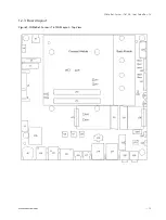
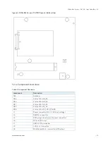
Page 14: ...COMe Ref Carrier i T6 TMI User Guide Rev 1 4 www kontron com 14 1 2 3 Board layout Figure 3 COMe Ref Carrier i T6 TMIP Layout Top View...

Page 15: ...Component Decsription C35 Goldcap D35 Status LED SUS_S3 D36 Status LED SUS_S4 D37 Status LED SUS_S5 D38 Status LED V12_S5 D39 Status LED V5 0_V3 3_PGOOD J1 Power connector 8 5V 30V input voltage J4 P...

Page 16: ...ctor J28 Mini PCIe card latch half size J29 COM port pin header COM2 SER1 J30 COM port pin header COM1 SER0 J31 SYS_Signals embedded interfaces pin header J32 GPIO pin header J33 SATA receptacle conne...

Page 17: ...l size card slot muxed with SATA 1 mSATA and connected to the SIM card slot J21 PCIe 2 for the onboard Gigabit Ethernet controller SATA Four SATA 6 Gb s interfaces SATA 0 via the 22 pin SATA plug conn...

Page 18: ...onnector J4 LEDs Two status LEDs available via the front panel connector J27 Power LED HDD Activity LED Switch Dip Switch One 8 position DIP switch SW1 for board configuration System Interfaces Power...

Page 19: ...00 00 5 COMe Mount Kit 5 mm 100 sets Mounting Kit for 100 modules including screws for 5 mm connectors 38017 0000 00 0 COMe Mount Kit 8 mm 1 set Mounting Kit for 1 module including screws for 8 mm con...

Page 20: ...n electrical and electronic equipment Environmental Vibration Sinusoidal IEC60068 2 6 Test parameters 9 150 Hz frequency range 1 g acceleration 1 oct min sweep rate 10 cycles axis 3 axes Single Shock...

Page 21: ...Rev 2 0 COM Express Module Base Specification Rev 2 1 SATA Serial ATA Specification Revision 3 0 PCI Express PCI Express Base Specification Rev 2 0 PCI Express M 2 Specification Rev 1 0 DisplayPort Di...

Page 22: ...an external Carrier BIOS Depending on the COMe module used the recommended SPI flash ICs include Winbond W25Q64FVSSIG 8 MB W25Q128FVSIG 16 MB Booting from the Carrier SPI flash can be enabled or disab...

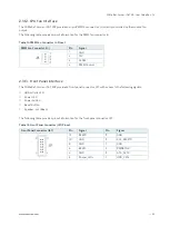
Page 23: ...e via the LVDS JILI connector J8 The following table provides pinout information for the LVDS JILI connector J8 Table 7 LVDS JILI Connector J8 Pinout LVDS JILI Connector J8 Pin Signal Pin Signal 1 LVD...

Page 24: ...COMe Ref Carrier i T6 TMI User Guide Rev 1 4 www kontron com 24 2 2 3 PEG Lanes The COMe Ref Carrier i T6 TMIP provides four PEG lanes PEG 0 3 used for the M 2 socket J34 PEG 0 is muxed with SATA 2...

Page 25: ...ICs U6 and U8 for the SATA 2 5 HDD mounting 2 3 3 M 2 Interface The COMe Ref Carrier i T6 TMIP provides an M 2 socket J34 via PEG 0 3 and SATA 2 muxed with PEG 0 which supports 3M key pinning and 2242...

Page 26: ...B 3 0 2 0 Pin Header J7 Pinout USB 3 0 2 0 Pin Header J7 Pin Signal Pin Signal 1 Power 20 2 SSRX2 19 Power 3 SSRX2 18 SSRX3 4 GND 17 SSRX3 5 SSTX2 16 GND 6 SSTX2 15 SSTX3 7 GND 14 SSTX3 8 USB2 13 GND...

Page 27: ...owing table provides pinout information for the pin headers J30 COM1 SER0 and J29 COM2 SER1 Table 11 Pin Headers J30 COM1 SER0 and J29 COM2 SER1 Pinouts COM SER Pin Headers J30 J29 Pin Signal J30 Sign...

Page 28: ...COMe Ref Carrier i T6 TMIP a pin header for various SYS_Signals embedded interfaces J31 is available and provides access to the following I Os I2C SMBus Watchdog LID SLEEP The following table provides...

Page 29: ...ector J4 Pin Signal 1 GND 2 12V 3 SENSE 4 PWM Control 2 3 13 Front Panel Interface The COMe Ref Carrier i T6 TMIP provides a front panel connector J27 with access to the following signals HDD activity...

Page 30: ...ts OFF Disable 5V standby power to USB ports USB 0 1 for wake events 5 ON Enable mSATA on full size Mini PCIe mSATA interface OFF Disable mSATA on full size MiniPCIe mSATA interface 6 ON Enable bootin...

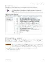
Page 31: ...nal 1 V_IN 2 V_IN 3 GND 4 GND The following mating power connectors are recommended for use with the COMe Ref Carrier i T6 TMIP Wurth Electronics Part Numbers 691361100004 691363110004 TE Connectivity...

Page 32: ...equipment is repaired or replaced within the stipulated warranty period Follow these steps before returning any product to Kontron 1 Visit the RMA Information website http www kontron com support and...

Page 33: ...r region s General Terms and Conditions of Sale 4 1 Limitation Exemption from Warranty Obligation In general Kontron shall not be required to honor the warranty even during the warranty period and sha...

Page 34: ...rcuit Communications IOT Internet of Things IPMI Intelligent Platform Management Interface ISA Industry Standard Architecture LAN Local Area Network LPC Low Pin Count Interface LVDS Low Voltage Differ...

Page 35: ...plications With its standard products and tailor made solutions based on highly reliable state of the art embedded technologies Kontron provides secure and innovative applications for a variety of ind...

Reviews: